Near Field Notes

Note 33PowerRev 1Watch the video · 2:22

Back-powering

Why does a switched-off sensor still draw 1 mA?

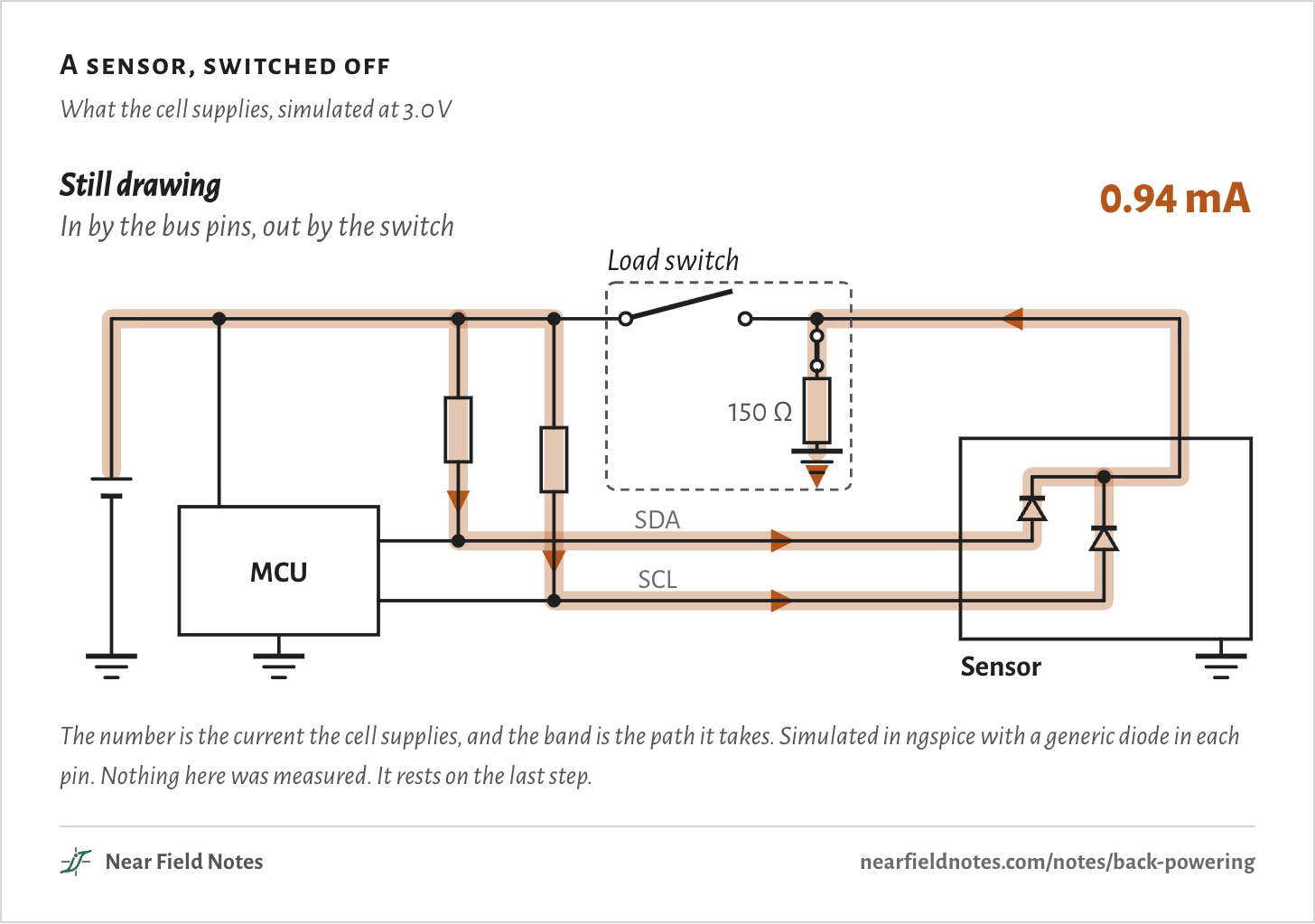
Because its I2C pins power it. With the bus pull-ups on a rail that stays on, current runs through them into the sensor’s SDA and SCL pins, up the protection diodes to its dead supply rail, and out through the load switch’s discharge resistor. Simulated on a 3.0 V coin cell board that comes to 0.94 mA, enough to empty a 225 mAh cell in 10 days.

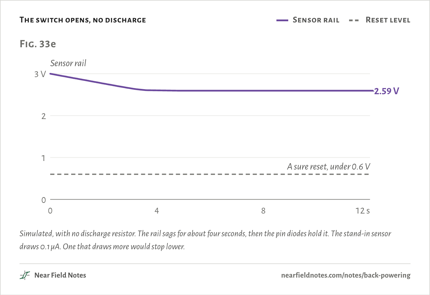
Take the discharge resistor away and the current stops. The pins then hold the sensor’s rail at 2.6 V, so cutting its power no longer resets it.

Of 23 common I2C sensors, 13 have the diode, going by their own datasheets. One line in the absolute-maximum table tells which.

A sensor, switched off

What the cell supplies, simulated at 3.0 V

Sensor onAsleep between readings0.13 µASensor switched offThe load switch opensStill drawingIn by the bus pins, out by the switch0.94 mAMCUSCLSDASensor150 ΩLoad switchSensor onAsleep between readings0.13 µASensor switched offThe load switch opensStill drawingIn by the bus pins, out by the switch0.94 mAMCUSCLSDASensor150 ΩLoad switchSensor onAsleep between readings0.13 µASensor switched offThe load switch opensStill drawingIn by the bus pins, out by the switch0.94 mAMCUSCLSDASensor150 ΩLoad switch
The number is the current the cell supplies, and the band is the path it takes. Simulated in ngspice with a generic diode in each pin. Nothing here was measured. It rests on the last step.

A coin cell board that switches its sensors off

44 × 24 mm, 3.0 V

Take a Bluetooth sensor board on a CR2032 coin cell. Its microcontroller wakes now and then, reads two sensors over I2C, sends the numbers and goes back to sleep.

To save the cell, a load switch cuts the sensors’ supply between readings. The microcontroller stays powered, and so do the two 4.7 kΩ pull-up resistors on SDA and SCL.

That leaves two lines held at 3.0 V, wired to chips that have no supply.

The board, and where the current leaks
  • Always-on rail
  • SDA, SCL
  • Sensor rail
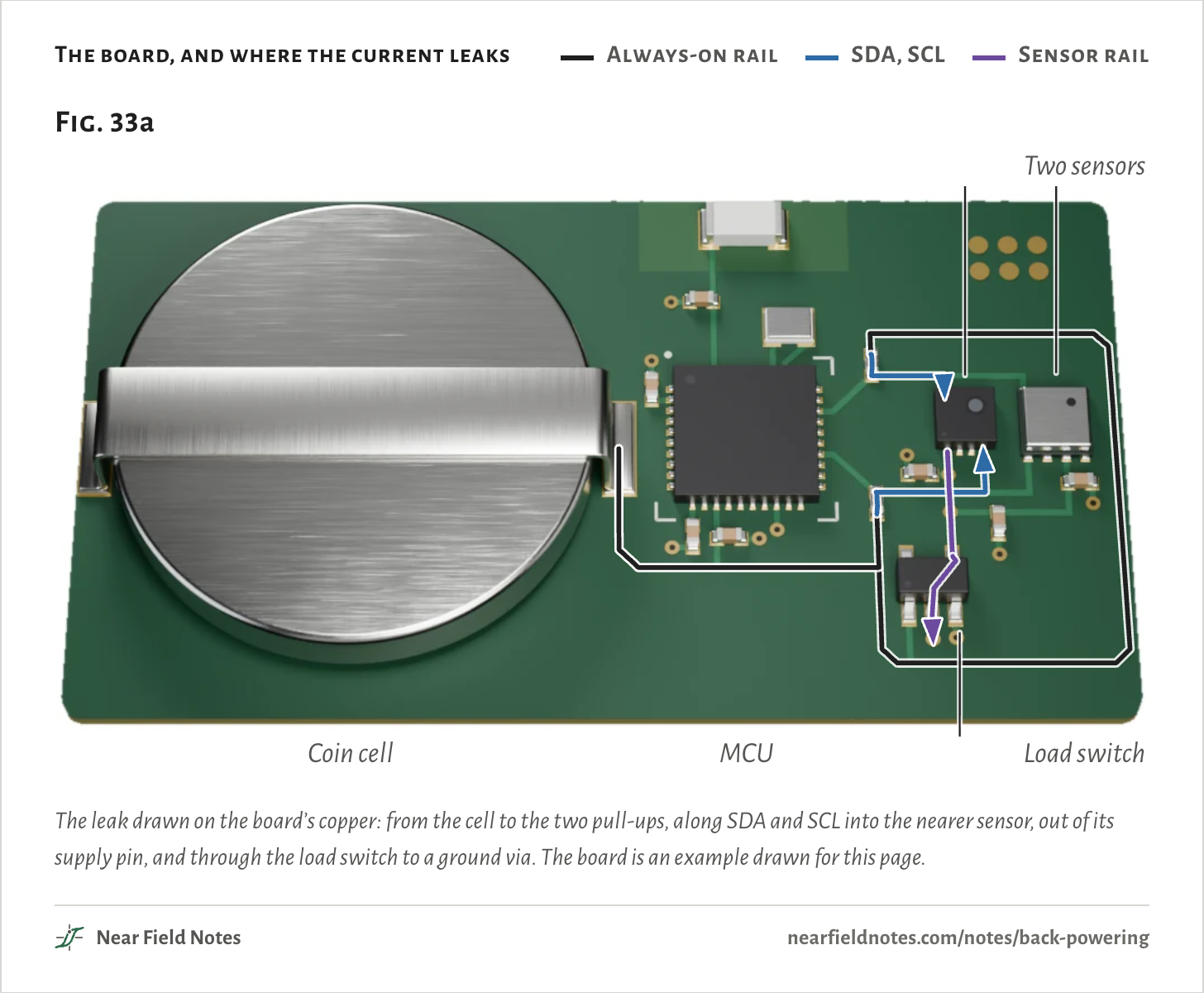
Fig. 33aCoin cellMCULoad switchTwo sensorsFig. 33aCoin cellMCULoad switchTwo sensorsFig. 33aCoin cellMCULoad switchTwo sensors
The leak drawn on the board’s copper: from the cell to the two pull-ups, along SDA and SCL into the nearer sensor, out of its supply pin, and through the load switch to a ground via. The board is an example drawn for this page.
The numbers
PartWhat it is
Coin cellA CR2032 under a retainer strap, 3.0 V. The always-on rail starts at the strap’s foot
MCUA Bluetooth microcontroller with its crystal and chip antenna. It stays powered
Pull-upsTwo 4.7 kΩ resistors, one on SDA and one on SCL, both to the always-on rail
SensorsA temperature and humidity sensor and an air sensor, both on the same two bus lines and the same switched rail
Load switchFeeds the sensor rail. When it is off, a 150 Ω resistor inside it ties that rail to ground
Drawn pathBlack: the always-on rail. Blue: SDA and SCL. Purple: the sensor rail, through the switch to ground. Through one sensor only

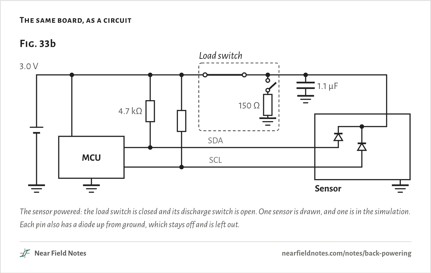
As a circuit, the cell feeds a rail that is always on. The microcontroller and both pull-ups hang from it. The load switch passes it on to the sensor’s supply pin, which has 1.1 µF of decoupling.

Two parts matter later. Inside the load switch, a resistor ties the sensor’s rail to ground whenever the switch is off, to bring the rail down quickly. TI calls it quick output discharge, and in its TPS22916 it is typically 150 Ω.

And inside the sensor, each bus pin has a protection diode that points up to the supply pin. It is part of the pin’s guard against static.

The same board, as a circuit
Fig. 33bMCUSCLSDASensor150 ΩLoad switch3.0 V4.7 kΩ1.1 µFFig. 33bMCUSCLSDASensor150 ΩLoad switch3.0 V4.7 kΩ1.1 µFFig. 33bMCUSCLSDASensor150 ΩLoad switch3.0 V4.7 kΩ1.1 µF
The sensor powered: the load switch is closed and its discharge switch is open. One sensor is drawn, and one is in the simulation. Each pin also has a diode up from ground, which stays off and is left out.

How the current gets in

A diode in each pin

An I2C line idles high. No chip drives it there. A pull-up resistor holds it at the rail’s voltage, and any chip on the bus can pull it low, which is why the pull-up sets the bus’s pace in Note 24.

While the sensor has power, its pin diodes do nothing. The pin is at 3.0 V and so is the supply, so no voltage sits across them.

Open the load switch and the sensor’s supply falls. The pull-ups still hold the pins at 3.0 V. Once a pin is a diode drop above the supply, the diode conducts. Current runs from the cell through the pull-up, into the pin and onto the sensor’s own rail.

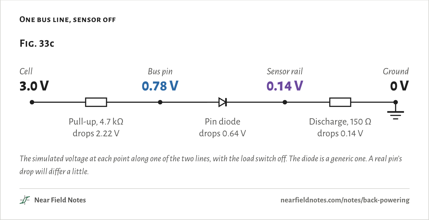
That is back-powering: a chip fed through a signal pin while its supply pin is off. The pull-up sets how much. In the simulation each line carries 0.47 mA.

One bus line, sensor off
Fig. 33cCell3.0 VBus pin0.78 VSensor rail0.14 VGround0 VPull-up4.7 kΩdrops 2.22 VPin diodedrops 0.64 VDischarge150 Ωdrops 0.14 VFig. 33cCell3.0 VBus pin0.78 VSensor rail0.14 VGround0 VPull-up, 4.7 kΩdrops 2.22 VPin diodedrops 0.64 VDischarge, 150 Ωdrops 0.14 VFig. 33cCell3.0 VBus pin0.78 VSensor rail0.14 VGround0 VPull-up, 4.7 kΩdrops 2.22 VPin diodedrops 0.64 VDischarge, 150 Ωdrops 0.14 V
The simulated voltage at each point along one of the two lines, with the load switch off. The diode is a generic one. A real pin’s drop will differ a little.

The discharge resistor lets it out

150 Ω to ground

Where the current goes next depends on the load switch. With the switch off, its discharge resistor ties the sensor’s rail to ground through 150 Ω. Whatever comes in through the pins runs straight out again, for as long as the sensor is off.

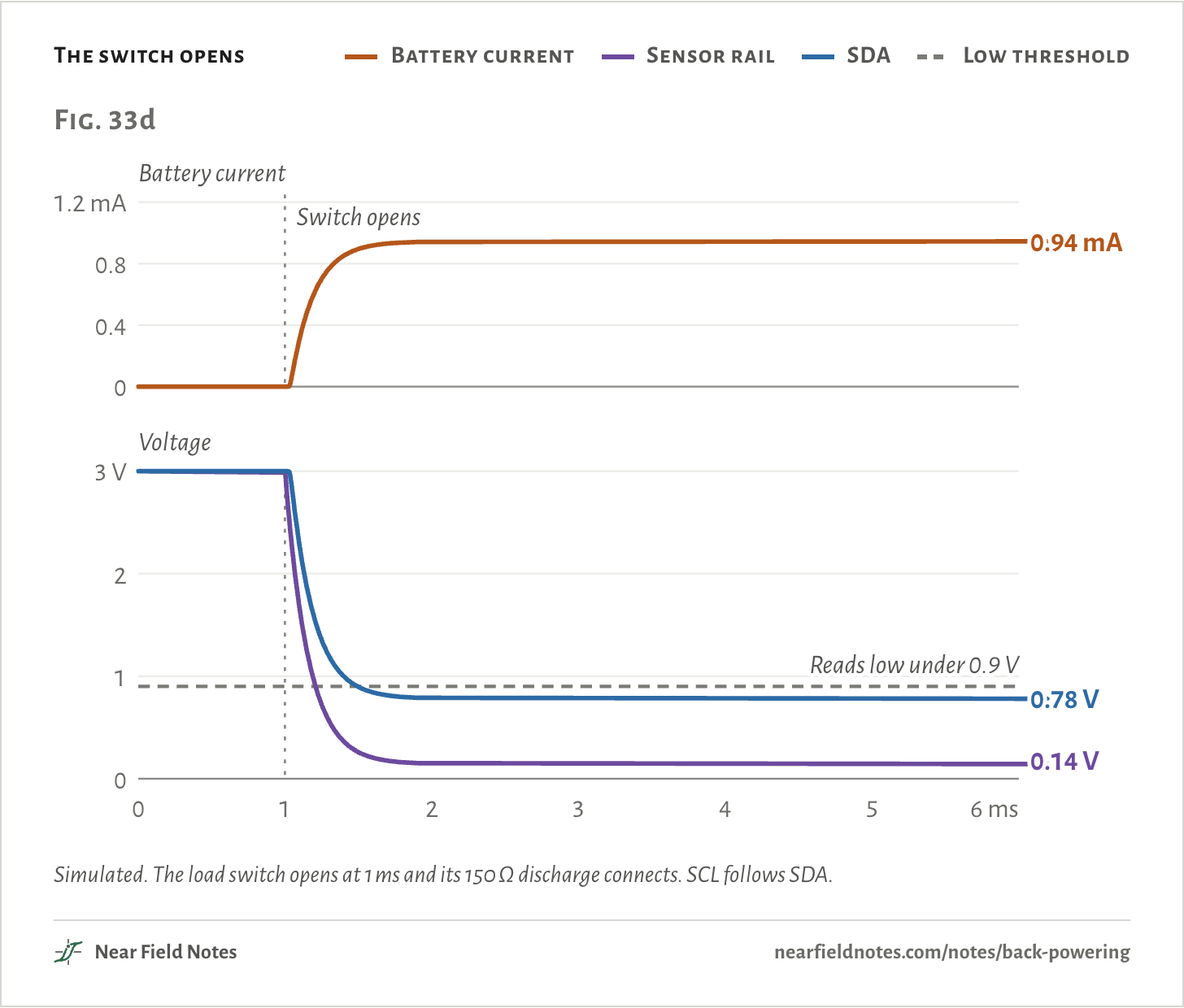
In the simulation the cell supplies 0.13 µA with the sensor on and asleep. Switch the sensor off and it supplies 0.94 mA. A 225 mAh coin cell that averages 10 µA lasts about 2.6 years. At 0.94 mA it lasts 10 days.

The switch opens
  • Battery current
  • Sensor rail
  • SDA
  • Low threshold
Fig. 33dBattery current00.40.81.2 mA0.94 mASwitch opensVoltage0123 VReads low under 0.9 V0.78 V0.14 V0123456 msFig. 33dBattery current00.40.81.2 mA0.94 mASwitch opensVoltage0123 VReads low under 0.9 V0.78 V0.14 V0123456 msFig. 33dBattery current00.40.81.2 mA0.94 mASwitch opensVoltage0123 VReads low under 0.9 V0.78 V0.14 V0123456 ms
Simulated. The load switch opens at 1 ms and its 150 Ω discharge connects. SCL follows SDA.
The numbers
3.0 V cell, 4.7 kΩ pull-ups, 150 Ω discharge. Settled values, switch open.
Simulated
Battery current, switch closed0.13 µA
Battery current, switch open944.4 µA
Sensor rail0.143 V
SDA and SCL0.781 V
An I2C input reads low under0.9 V, 0.3 × the supply
Rail under 1.5 V after0.12 ms
Rail under 0.6 V after0.29 ms
A 225 mAh cell lasts9.9 days
596

Without a discharge, the sensor can’t reset

The rail stops at 2.6 V

Some load switches have no discharge resistor, and on others it is a pin that can be left open. With no way to ground, the leak stops. The simulated battery current is 0.13 µA.

The rail has no way down either. It sags until the pin diodes start to conduct, and then they hold it up. In the simulation it stops at 2.6 V, a diode drop under the bus.

A sensor resets when its supply falls under a set level. For its SHT4x, Sensirion puts that level between 0.6 and 1.08 V, so a reset is only sure under 0.6 V. The rail never gets there. Switching the power off and on again can’t recover a sensor that has hung.

The switch opens, no discharge
  • Sensor rail
  • Reset level
Fig. 33eSensor rail0123 VA sure reset, under 0.6 V2.59 V04812 sFig. 33eSensor rail0123 VA sure reset, under 0.6 V2.59 V04812 sFig. 33eSensor rail0123 VA sure reset, under 0.6 V2.59 V04812 s
Simulated, with no discharge resistor. The rail sags for about four seconds, then the pin diodes hold it. The stand-in sensor draws 0.1 µA. One that draws more would stop lower.
The numbers
3.0 V cell, 4.7 kΩ pull-ups, no discharge. The stand-in sensor draws 0.1 µA above 1.0 V.
After the switch opensSensor rail
0 s3.00 V
1 s2.88 V
2 s2.77 V
3 s2.66 V
4 s2.61 V
5 s2.59 V
8 s2.59 V
12 s2.59 V
Battery current, settled0.13 µA
SDA and SCL, settled3.000 V
Against the discharge resistor’s value
  • Reset level
Fig. 33fBattery current00.40.81.2 mA0.940.710.19Sensor rail0123 VA sure reset, under 0.6 V0.140.711.9524 Ω1501 k10 k100 k1 MΩFig. 33fBattery current00.40.81.2 mA0.940.710.19Sensor rail0123 VA sure reset, under 0.6 V0.140.711.9524 Ω1501 k10 k100 k1 MΩFig. 33fBattery current00.40.81.2 mA0.940.710.19Sensor rail0123 VA sure reset, under 0.6 V0.140.711.9524 Ω1501 k10 k100 k1 MΩ
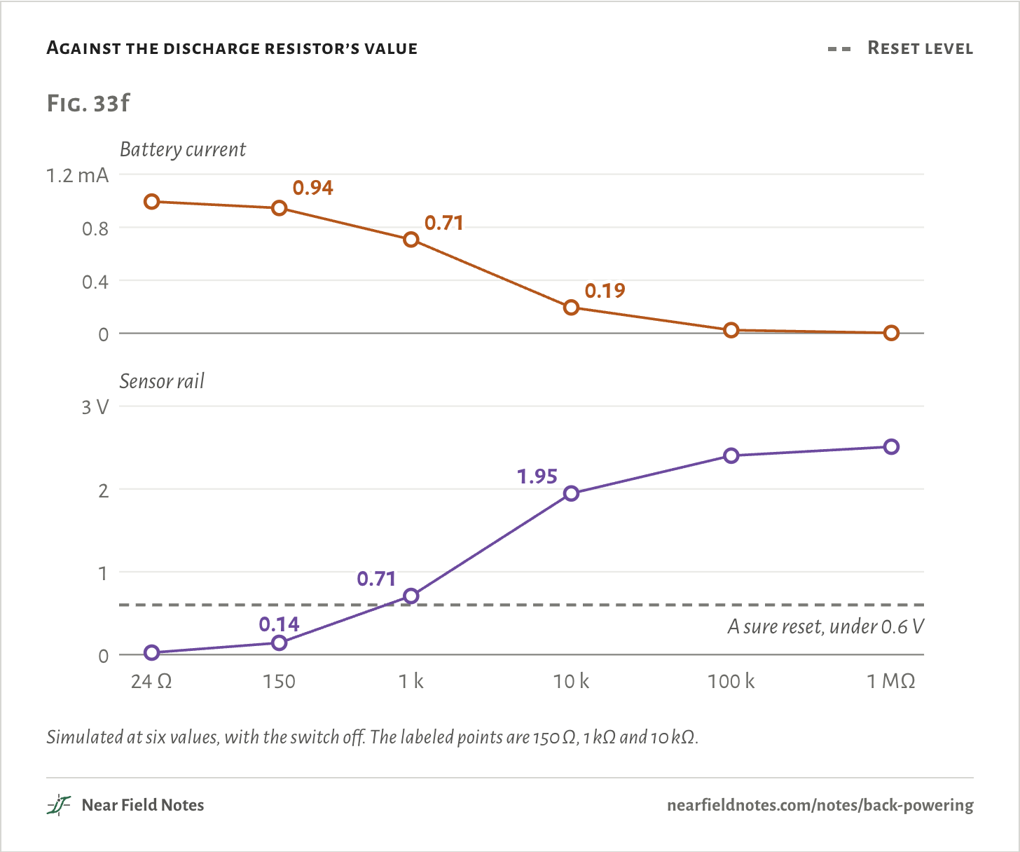
Simulated at six values, with the switch off. The labeled points are 150 Ω, 1 kΩ and 10 kΩ.
The numbers
3.0 V cell, 4.7 kΩ pull-ups, switch open. Cell life is for 225 mAh and counts this current alone.
DischargeCurrentRailSDABus readsCell life
24 Ω0.99 mA0.025 V0.664 VLow9.4 days
150 Ω0.94 mA0.143 V0.781 VLow9.9 days
1 kΩ0.71 mA0.708 V1.338 VNeither13.3 days
10 kΩ0.19 mA1.947 V2.542 VHigh48.1 days
100 kΩ24 µA2.402 V2.943 VHigh388 days
1 MΩ2.64 µA2.510 V2.994 VHigh10 years
None0.13 µA2.595 V3.000 VHighOver 10 years
598

What the spec says, and 23 datasheets

13 tied to the supply, 8 fixed

The I2C specification covers this. NXP’s UM10204 has a note on its table of electrical limits: “If VDD is switched off, I/O pins of Fast-mode and Fast-mode Plus devices must not obstruct the SDA and SCL lines.” SMBus asks more. An unpowered device has to provide “protection against back powering the SMBus”.

Many sensors have the diode anyway, and the datasheet shows it. Find the bus pins in the absolute-maximum table. If the most they may see is the supply plus 0.3 V, a diode runs from the pin to the supply. If it is a fixed voltage, like 6 V, there is none. TI’s guide to reading its logic datasheets gives the same rule.

23 I2C sensors, by their datasheets

Fig. 33g

Rating on SDA, SCLSensors
Tied to the supply: 13 sensors
VDDIO + 0.3 VBME280, BME688, BMI270, BMP390, LIS2DH12, LPS22HB, LPS22HH, LSM6DSO
VDD + 0.3 VHTS221, SCD4x, SHT3x, SHT4x
VDDIO + 0.5 VICM-42688-P
A fixed voltage: 8 sensors
6 VHDC3020, MAX30102, MCP9808, OPT3001, TMP117
6.5 VPCT2075
3.9 VHDC2080
3.6 VENS160
No rating given: 2
Not statedSGP40, SGP41, VEML7700
The absolute-maximum rating each datasheet gives for SDA and SCL. A rating tied to the supply means a diode to it. ST writes VDDIO as Vdd_IO.
The numbers
From each datasheet’s absolute-maximum table, read in November 2026. The words are paraphrased.
SensorMaximum on SDA and SCLWhat else it says
Bosch BME280VDDIO + 0.3 VProhibits holding a pin high with VDDIO switched off
Bosch BME688VDDIO + 0.3 VSays both pads have diodes to VDDIO
Bosch BMP390VDDIO + 0.3 VSays a pin held high with VDDIO off can damage the part
Bosch BMI270VDDIO + 0.3 V, under 4 VSays to keep the pins near ground with VDDIO off
Sensirion SHT4xVDD + 0.3 VA reset by power-down includes pulling SCL and SDA low
Sensirion SHT3xVDD + 0.3 VSays the pins’ voltage has to go too, or the diodes power it
Sensirion SCD4xVDD + 0.3 V
Sensirion SGP40, SGP41Not statedOnly the supply pins are rated
TI TMP1176 V
TI HDC20803.9 VIts DRDY/INT pin is rated to VDD + 0.3 V
TI HDC30206.0 VADDR1, ALERT and RESET are rated to VDD + 0.3 V
TI OPT30016 VAllows a pull-up rail above VDD
ST LIS2DH12Vdd_IO + 0.3 V
ST LSM6DSOVDDIO + 0.3 V
ST LPS22HBVdd_IO + 0.3 V
ST LPS22HHVdd_IO + 0.3 V
ST HTS221VDD + 0.3 V
ScioSense ENS1603.6 VADDR, INTn and CSn are rated to VDDIO + 0.3 V
Vishay VEML7700Not statedOnly the supply pin is rated
TDK ICM-42688-PVDDIO + 0.5 V
Analog Devices MAX301026.0 VSays the pins can be pulled up with its supplies off
Microchip MCP98086.0 V
NXP PCT20756.5 VSays SDA can be pulled up whatever the supply. Address pins are rated to VCC + 0.3 V
600

Ways to stop it

The same circuit, sensor off

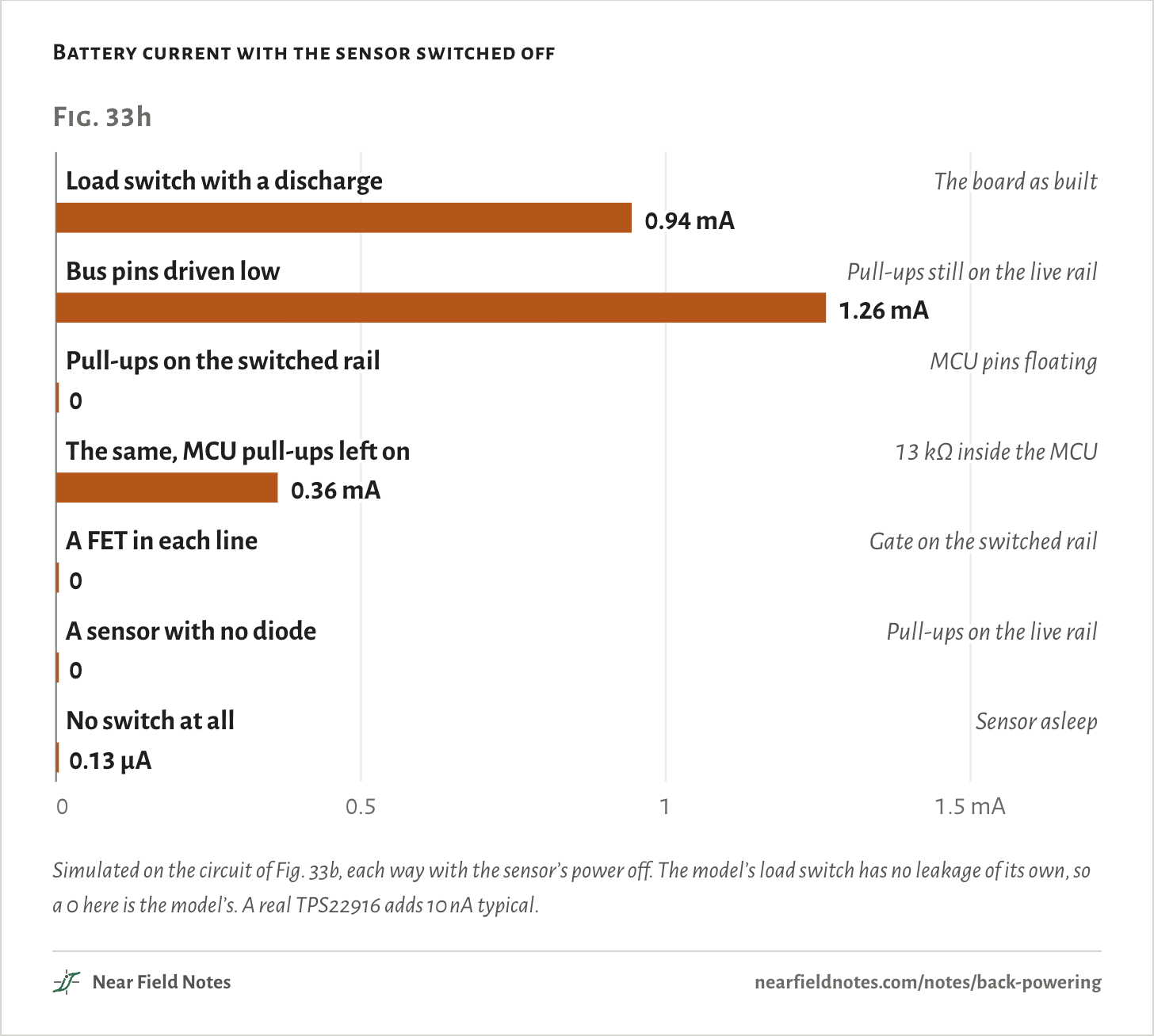
Driving SDA and SCL low before the switch opens looks right, since it takes the voltage off the pins. With the pull-ups still on the live rail it is worse. Each pull-up now has the whole 3.0 V across it, and the cell supplies 1.26 mA.

Moving the pull-ups to the switched rail works. They lose their supply with the sensor, nothing holds the bus up, and the simulated current is 0.

The microcontroller’s pins have to float, though. Leave its internal pull-ups on and they feed the sensor’s pins in place of the resistors: 0.36 mA through 13 kΩ each. On Nordic’s nRF52832 and nRF52840 that is easy to do. Their product specifications say: “The PIN_CNF registers are retained registers.” A pull-up left enabled stays on through System OFF, the deepest sleep.

Battery current with the sensor switched off
Fig. 33h00.511.5 mALoad switch with a discharge0.94 mAThe board as builtBus pins driven low1.26 mAPull-ups still on the live railPull-ups on the switched rail0MCU pins floatingThe same, MCU pull-ups left on0.36 mA13 kΩ inside the MCUA FET in each line0Gate on the switched railA sensor with no diode0Pull-ups on the live railNo switch at all0.13 µASensor asleepFig. 33h00.511.5 mALoad switch with a discharge0.94 mAThe board as builtBus pins driven low1.26 mAPull-ups still on the live railPull-ups on the switched rail0MCU pins floatingThe same, MCU pull-ups left on0.36 mA13 kΩ inside the MCUA FET in each line0Gate on the switched railA sensor with no diode0Pull-ups on the live railNo switch at all0.13 µASensor asleepFig. 33h00.511.5 mALoad switch with a discharge0.94 mAThe board as builtBus pins driven low1.26 mAPull-ups still on the live railPull-ups on the switched rail0MCU pins floatingThe same, MCU pull-ups left on0.36 mA13 kΩ inside the MCUA FET in each line0Gate on the switched railA sensor with no diode0Pull-ups on the live railNo switch at all0.13 µASensor asleep
Simulated on the circuit of Fig. 33b, each way with the sensor’s power off. The model’s load switch has no leakage of its own, so a 0 here is the model’s. A real TPS22916 adds 10 nA typical.
The numbers
3.0 V cell, 4.7 kΩ pull-ups, 150 Ω discharge. The model’s switch has no leakage of its own. Cell life is for 225 mAh and counts this current alone.
WayCurrentRailSDA at the MCUCell life
Load switch with a discharge944.39 µA0.14 V0.78 V9.9 days
Bus pins driven low1263.16 µA0.00 V0.03 V7.4 days
Pull-ups on the switched rail0.00 µA0.00 V0.00 V—
Pull-ups on the switched rail, bus pins driven low0.00 µA0.00 V0.00 V—
The same, MCU pull-ups left on363.59 µA0.05 V0.64 V25.8 days
No resistors, only the MCU’s pull-ups, left on359.11 µA0.05 V0.67 V26.1 days
A FET in each line0.00 µA0.00 V3.00 V—
A sensor with no diode0.00 µA0.00 V3.00 V—
No switch at all0.13 µA3.00 V3.00 VOver 10 years

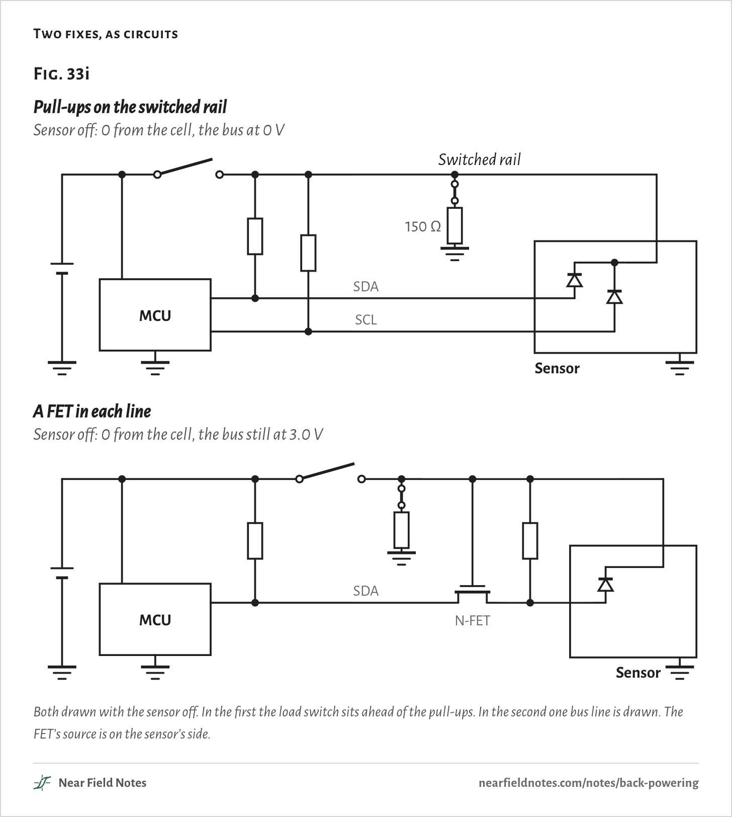
Pull-ups on the switched rail take the whole bus down with the sensor. If other chips share the bus and have to keep talking, put a small N-channel FET in each line, between the sensor and the rest of the bus, with its gate on the switched rail.

It is the usual level-shifter circuit. While the sensor has power, the FET passes the bus both ways. When the rail goes off, the gate goes with it and the sensor’s pins are cut off from the live bus. The simulated current is 0, and the microcontroller’s side of the bus stays at 3.0 V. The sensor’s side needs a pull-up of its own, to the switched rail.

The last way is to leave the switch out. A BME280 asleep draws 0.1 µA typical, which is 100 nA. A TPS22916 that is off still leaks 10 nA typical. Switching that sensor off saves about 90 nA.

Two fixes, as circuits
Fig. 33iPull-ups on the switched railSensor off: 0 from the cell, the bus at 0 VMCUSCLSDASensor150 ΩSwitched railA FET in each lineSensor off: 0 from the cell, the bus still at 3.0 VMCUN-FETSDASensorFig. 33iPull-ups on the switched railSensor off: 0 from the cell, the bus at 0 VMCUSCLSDASensor150 ΩSwitched railA FET in each lineSensor off: 0 from the cell, the bus still at 3.0 VMCUN-FETSDASensorFig. 33iPull-ups on the switched railSensor off: 0 from the cell, the bus at 0 VMCUSCLSDASensor150 ΩSwitched railA FET in each lineSensor off: 0 from the cell, the bus still at 3.0 VMCUN-FETSDASensor
Both drawn with the sensor off. In the first the load switch sits ahead of the pull-ups. In the second one bus line is drawn. The FET’s source is on the sensor’s side.

Switch it, and how?

Three questions

Which fix fits depends on three things: what the sensor draws asleep, what its datasheet rates the bus pins to, and what else is on the bus.

Key to a switched I2C sensor

Does it need a switch, and where do the pull-ups go?

  1. 1aAsleep, the sensor draws about what a load switch leaksNo switch
  2. 1bIts power has to be cutGo to 2
  3. 2aSDA and SCL are rated to a fixed voltage, like 6 VA load switch alone
  4. 2bThey are rated to the supply plus 0.3 VGo to 3
  5. 3aNothing else has to use the bus while the sensor is offPull-ups on the switched rail
  6. 3bOther chips share the busA FET in each line

The board in Fig. 33a ends at 3a: the microcontroller is the only other chip on its bus. Its pins then have to float while the sensors are off, with its own pull-ups disabled.

Conditions

Simulated
Every current and voltage on this page comes from a circuit simulation. None was measured on a board.
Circuit
A 3.0 V source for the cell. Two 4.7 kΩ pull-ups from the always-on rail to SDA and SCL, with 50 pF on each line. The bus is idle: nothing drives it.
Load switch
An ideal switch, 80 mΩ when on, with no leakage of its own. It opens at 1 ms. Its discharge is a 150 Ω resistor that connects when the switch is off, the typical value for TI’s TPS22916.
Sensor
One sensor on the bus, with 1.1 µF on its rail. Its supply draws 0.1 µA once the rail is above 1.0 V, plus 100 MΩ to ground. That is a stand-in for a sensor asleep. It has no reset behavior.
Pin diode
A generic junction diode from each bus pin up to the sensor’s rail, and one from ground up to each pin: 10 fA saturation current, ideality 1, 5 Ω in series, 2 pF. It is no maker’s model.
Microcontroller
Its pins are high-impedance, or pulled up through 13 kΩ, Nordic’s typical value, or driven low through 50 Ω.
FET
A level-1 N-channel model with a 1.0 V threshold and its body diode, one in each line, with a 4.7 kΩ pull-up on each side.
Solver
ngspice, 80 transient runs. Each settled number is an average over the last 5% of its run.
Cell life
225 mAh is assumed for the coin cell. Each life counts the leak alone, with the cell held at 3.0 V.
Reset level
0.6 V, the low end of the 0.6 to 1.08 V power-up/down level in Sensirion’s SHT4x datasheet.
Survey
23 I2C sensors, each read from its maker’s datasheet in November 2026. The SGP40 and SGP41 count as one. A fixed rating is a reading of the datasheet. No part was tested.
Render
Blender. The board is an example drawn for this page, with generic parts.

Simulated only. Nothing on this page has been measured on a board.

Limits

  • The pin diode is generic. It hardly moves the leak, but it moves where a rail with no discharge stops: 2.78 to 3.01 V at 3.3 V over four decades of saturation current.
  • The sensor’s load is a stand-in. A real part half-powered through its pins may draw far more than 0.1 µA, or wake up and drive the bus. None of that is modeled.
  • The board has two sensors and the simulation has one. A second would share the same two pull-ups, so the total should change little. That was not simulated.
  • The numbers are for 3.0 V and 4.7 kΩ. The pull-ups set the leak, so other values scale it.
  • A real cell sags as it drains, and the leak falls with it.
  • Whether back-powering harms a sensor is not covered here. Datasheets differ on it, and this page has no failure data.

Files

  • sim/backpower.pyThe ngspice circuit and every run: supply and pull-up values, discharge values, the diode, the fixes and the traces
  • research_notes/parts_survey.mdThe 23 sensors, the load switches and the microcontrollers, each with its datasheet’s wording
  • render/scene.pyThe board in Blender, with its routed traces

Sources

Like this note?

Rev 1 ·
  1. Rev 1First published

Each fix gets a line here, with the reader's name if they want credit.

Did it answer your question?

Want more on this?

Report a problem

What should the next note be? Ask for one