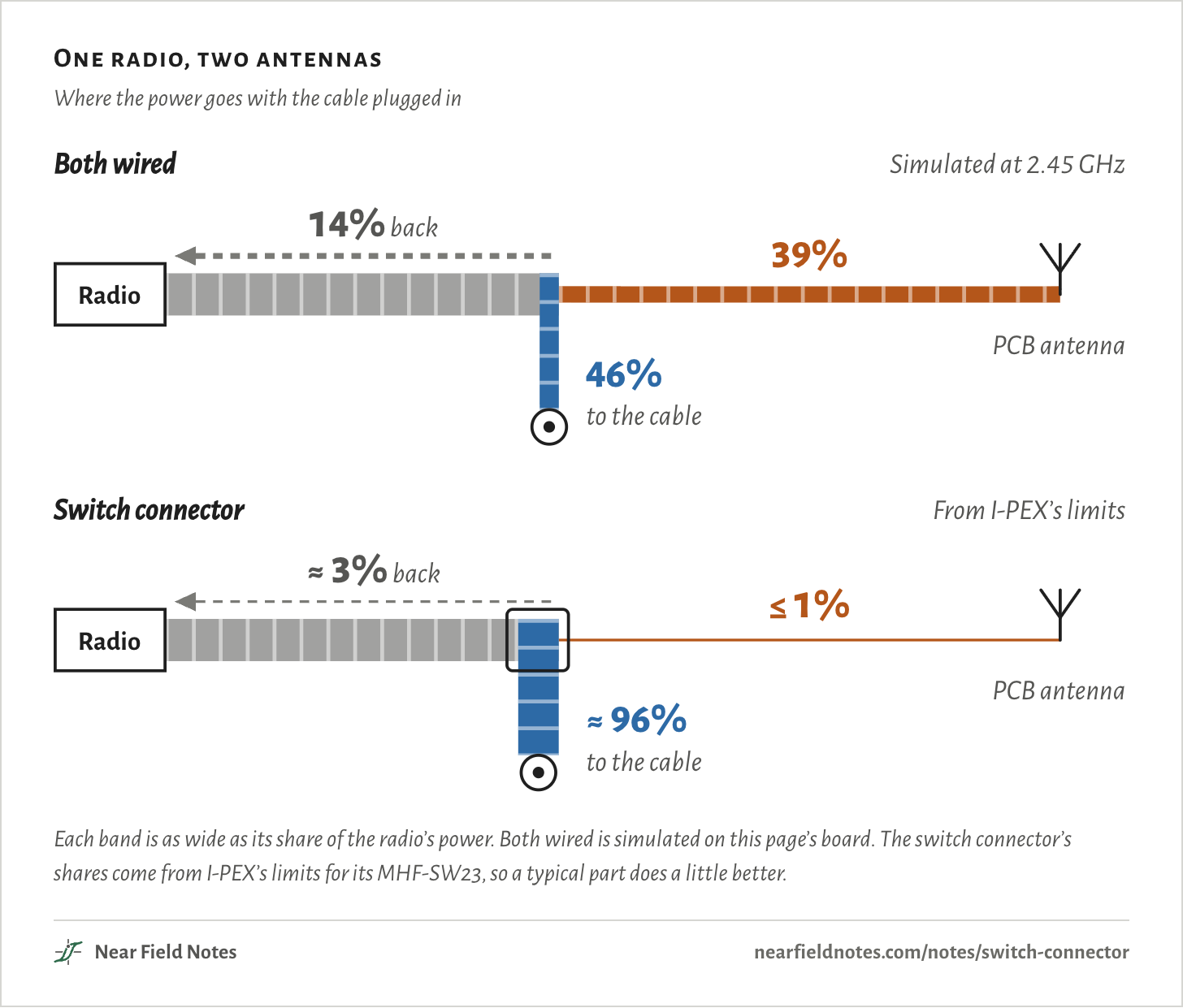
Because the power splits. With a PCB antenna and a cable both wired to the radio, 46% of its power reaches the cable, 39% goes to the PCB antenna and 14% bounces back. A switch connector sends about 96% to the cable, and it switches itself when the plug goes in.
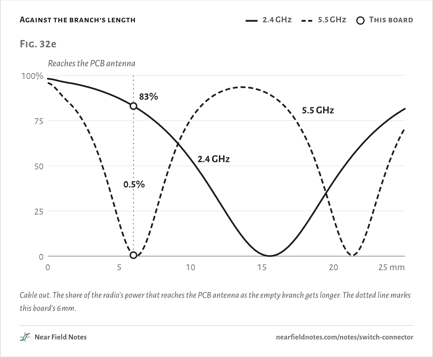
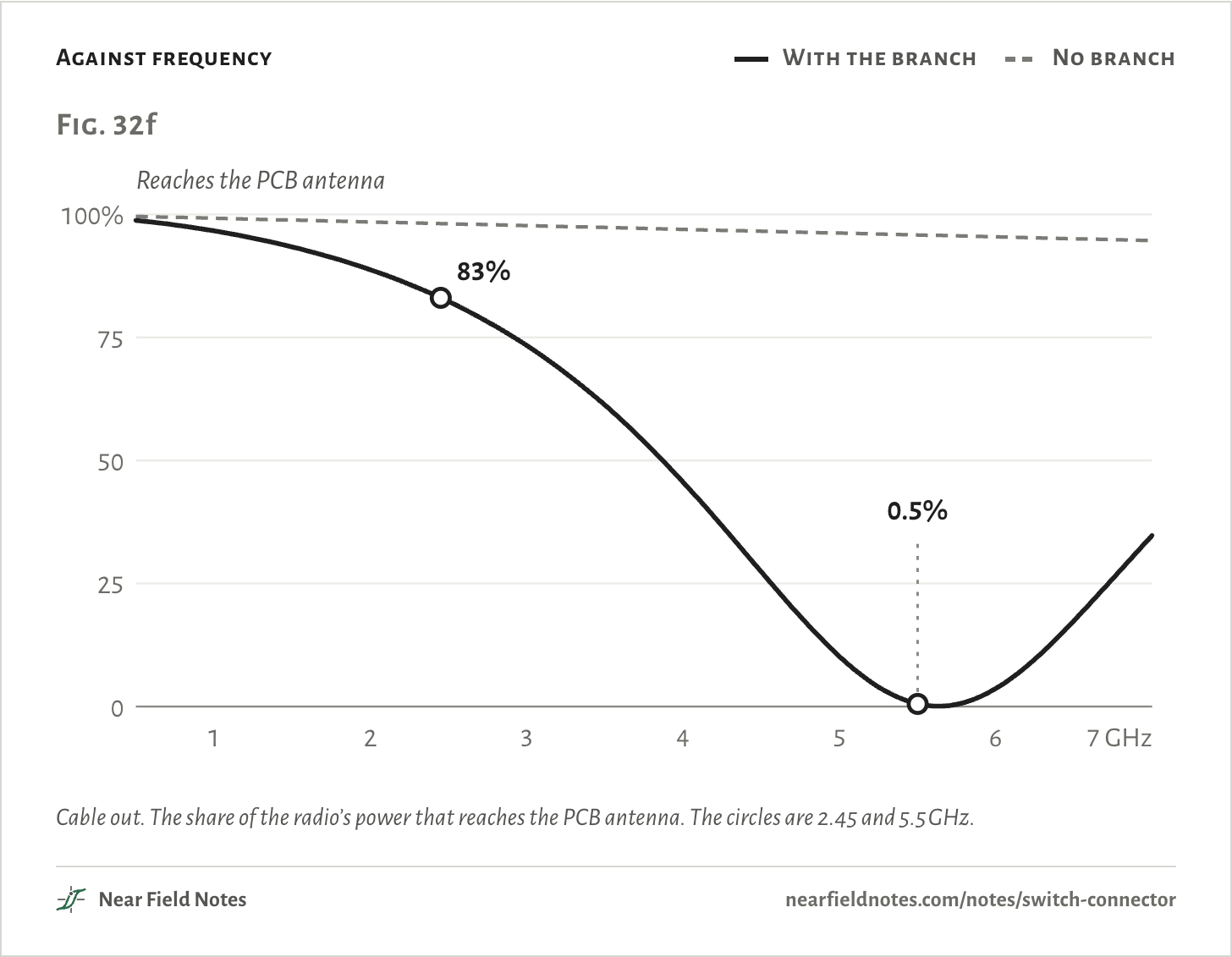
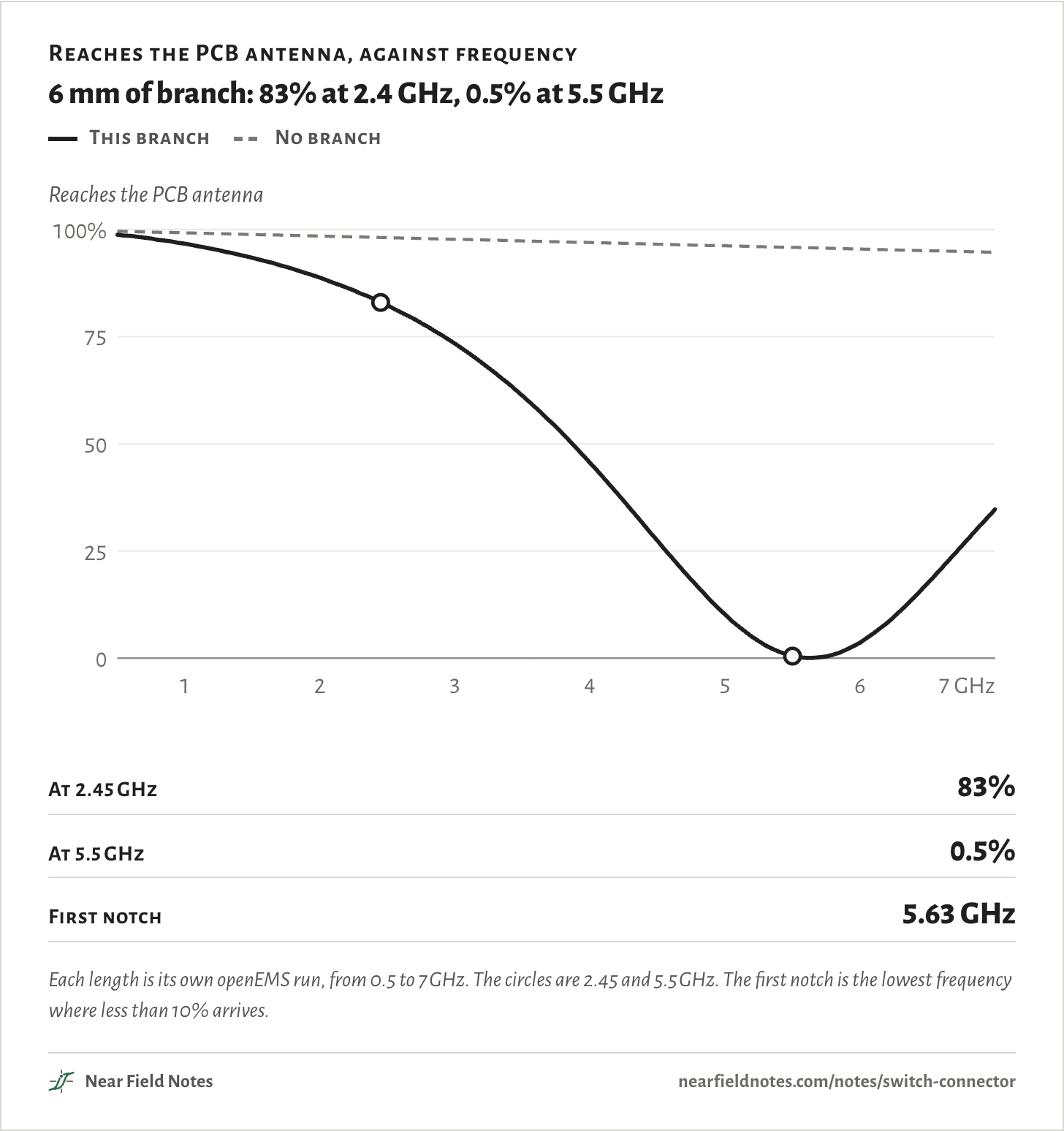
Unplug the cable and the empty branch still costs. On this board it lets 83% through to the PCB antenna at 2.4 GHz and 0.5% at 5.5 GHz.
A 0 Ω resistor or an RF switch chip can pick the antenna too. Each suits a different product.
One radio, two antennas
Where the power goes with the cable plugged in
Each band is as wide as its share of the radio’s power. Both wired is simulated on this page’s board. The switch connector’s shares come from I-PEX’s limits for its MHF-SW23, so a typical part does a little better.The numbers
Shares of the power the radio sends, with the cable plugged in. The switch connector’s row leaves out the board’s traces.
To the cable
To the PCB antenna
Back to the radio
Lost
Both wired, simulated at 2.45 GHz
45.6%
39.0%
14.1%
1.3%
Switch connector, I-PEX’s limits to 3 GHz
96.0% or more
1.0% at most
2.8% at most
0.2%, a 100 mΩ contact
The board and its two antennas
34 × 24 mm, 4 layers
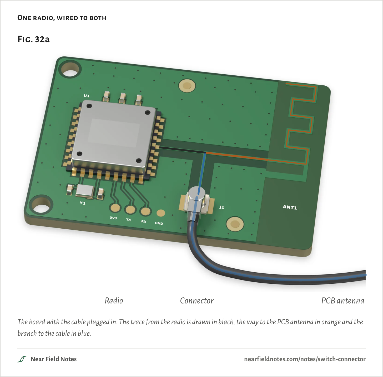
A 2.4 GHz radio module, U1, sits on the left of the board. Its PCB antenna, ANT1, is printed in the copper on the right. It is the meandered inverted-F from TI’s AN043, the antenna of Note 3.
J1 is a U.FL connector for an external antenna on a cable. A product like this ships with the PCB antenna working, and a cable goes in when it needs more range or sits inside a metal box.
The easy layout is a tee. One trace leaves the radio, and at a junction it goes both ways, so both antennas stay wired all the time.
One radio, wired to both
The board with the cable plugged in. The trace from the radio is drawn in black, the way to the PCB antenna in orange and the branch to the cable in blue.The numbers
Part
What it is
U1
2.4 GHz radio module under its shield
Y1
Its crystal
ANT1
PCB antenna: a meandered inverted-F printed in the top copper, the outline from TI’s AN043
J1
U.FL connector for an external antenna, with a 1.13 mm coax cable plugged in
Trace
50 Ω microstrip, 0.373 mm wide: 5.5 mm from the radio to the tee, 7.5 mm on to the PCB antenna, 6 mm down the branch to J1’s pad
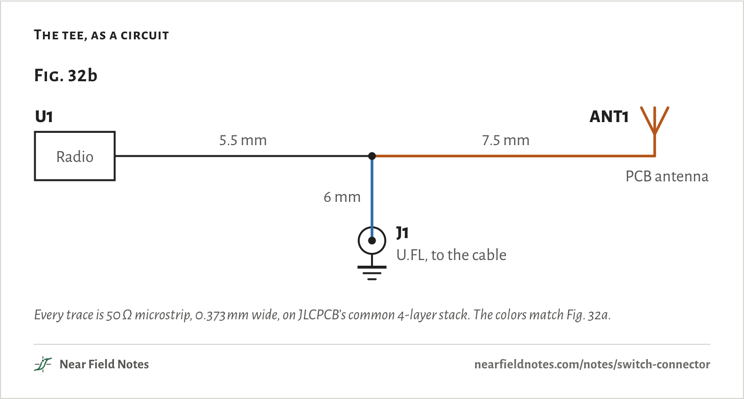
As a circuit it is three pieces of 50 Ω trace meeting at one point. The radio’s is 5.5 mm long. The PCB antenna is 7.5 mm past the junction, and J1’s pad is 6 mm down the branch.
That leaves two cases to check: the cable plugged in, and the cable out.
The tee, as a circuit
Every trace is 50 Ω microstrip, 0.373 mm wide, on JLCPCB’s common 4-layer stack. The colors match Fig. 32a.
Both wired, the power splits
Cable in, 2.45 GHz
At the junction the radio’s 50 Ω trace meets two 50 Ω loads side by side, and together they look like 25 Ω. A wave that meets a different impedance partly bounces back:
Γ=ZL−Z0ZL+Z0
=25 Ω − 50 Ω25 Ω + 50 Ω=−1/3
The share of the power that bounces is that number squared:
PbackP=Γ2
=(1/3)²=1/9=11.1%
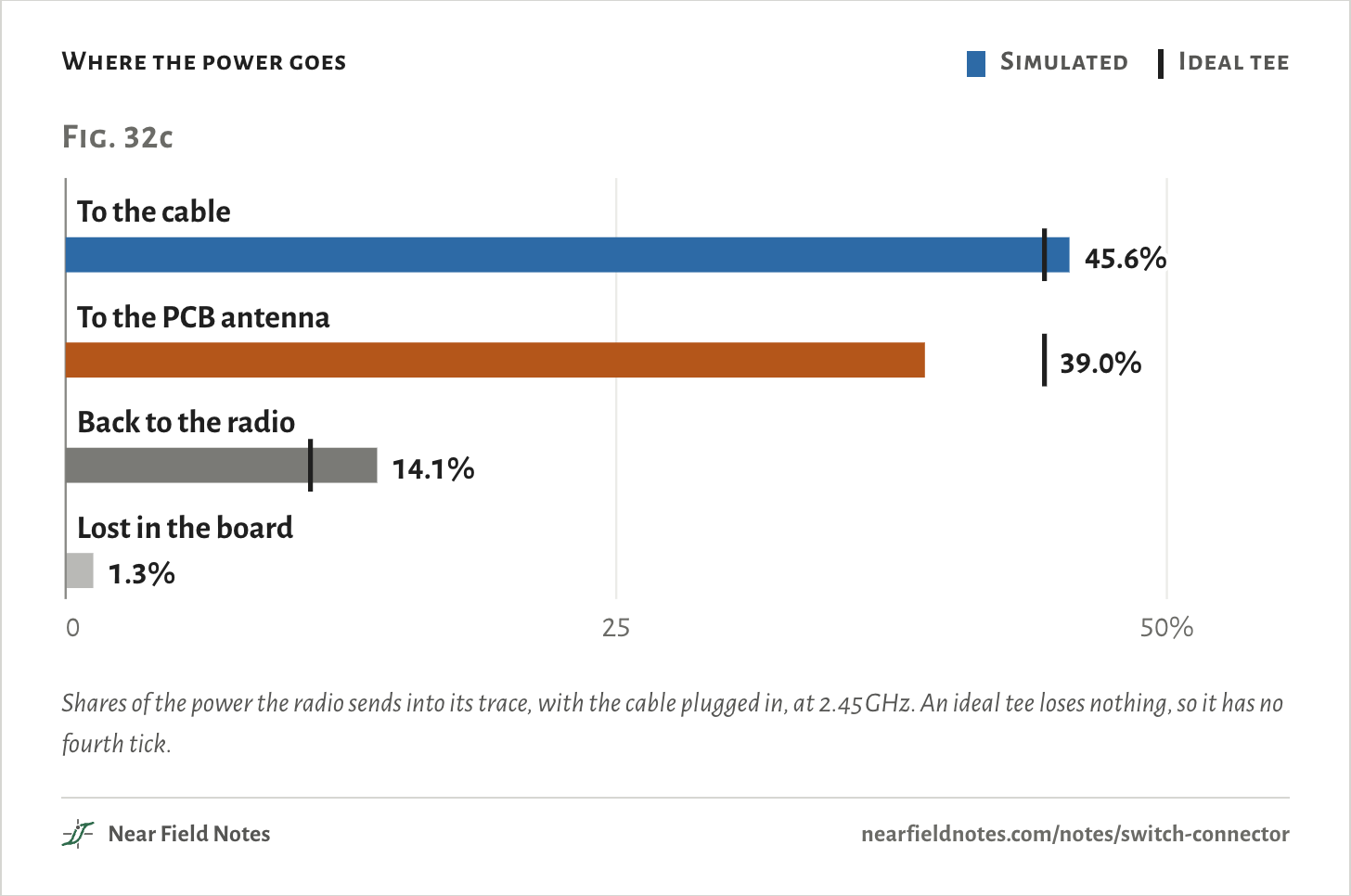
The other 88.9% splits evenly, 44.4% each way. That is an ideal tee. On the board, the branch ends in J1’s 1 × 1 mm pad, which is a small capacitor to the ground under it. It makes the branch look lower than 50 Ω, so the branch takes more than its half and more bounces back.
Where the power goes
Simulated
Ideal tee
Shares of the power the radio sends into its trace, with the cable plugged in, at 2.45 GHz. An ideal tee loses nothing, so it has no fourth tick.The numbers
Shares of the power the radio sends into its trace, cable plugged in.
Cable
PCB antenna
Back
Lost
Ideal tee, two 50 Ω loads
44.4%
44.4%
11.1%
0
Simulated, 2.45 GHz
45.6%
39.0%
14.1%
1.3%
Simulated, 5.5 GHz
44.8%
36.6%
15.0%
3.6%
Same tee without J1’s pad, 2.45 GHz
43.6%
43.6%
11.5%
1.3%
A 50 Ω line past the pad as the cable, 2.45 GHz
45.2%
40.0%
13.5%
1.3%
Finer mesh, 2.45 GHz
45.6%
39.0%
14.1%
1.3%
590
Tee junction
46% to the cable, 39% to the other antenna
Field marks. With the cable in, 46% of the radio’s power reaches it. 39% goes to the PCB antenna, 14% bounces back to the radio and 1.3% is lost in the board.
Look-alike. A 3 dB splitter. A tee is said to cost half the power. It costs a little more, because it reflects as well as splits: an ideal tee delivers 44.4% each way, 3.5 dB down.
Range. At 5.5 GHz the split is 45% to the cable, 37% to the PCB antenna and 15% back. The same tee without J1’s pad gives 43.6%, 43.6% and 11.5% at 2.45 GHz, close to the ideal.
Habitat. Boards that offer a PCB antenna and a connector, and leave both wired so nothing has to be chosen at the factory.
591
Cable out, the branch is a stub
Nothing plugged in
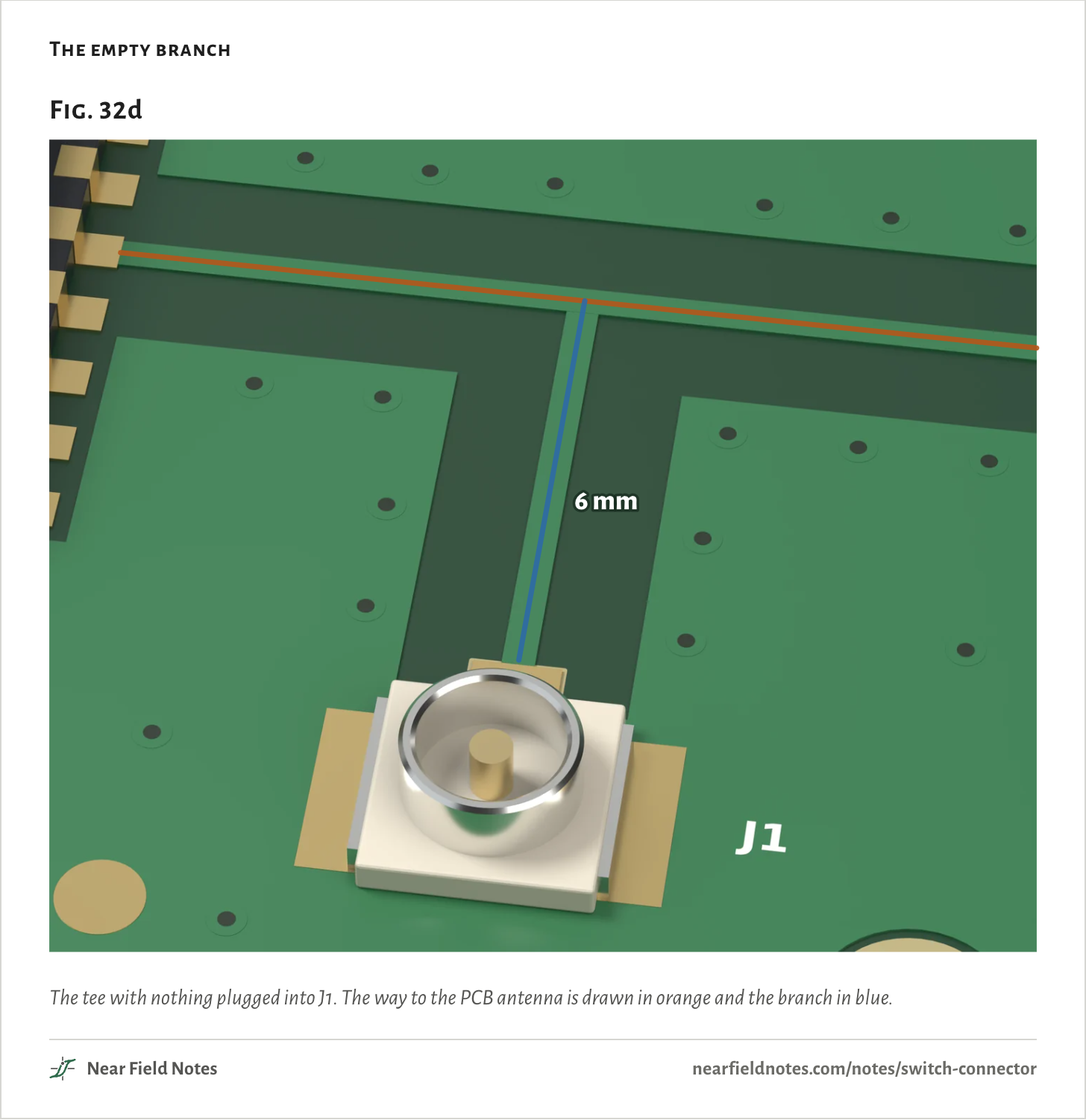
Unplug the cable and the branch ends at J1’s empty pad. A trace that leads nowhere is a stub. The wave runs down it, bounces off the open end and comes back to the junction.
When the trip down and back takes half a cycle, the returning wave cancels the one at the junction. The junction then looks like a short, and nearly all of the power bounces back to the radio. That happens when the stub is a quarter of a wavelength long:
L¼=c4fεeff
=3.00 × 10⁸ m/s4 × 5.5 GHz × 3.23=7.58 mm
J1’s pad makes the stub act 1.4 mm longer than its trace, so at 5.5 GHz the dip comes at 6.2 mm of branch. This board’s branch is 6 mm.
The empty branch
The tee with nothing plugged into J1. The way to the PCB antenna is drawn in orange and the branch in blue.
Against the branch’s length
2.4 GHz
5.5 GHz
This board
Cable out. The share of the radio’s power that reaches the PCB antenna as the empty branch gets longer. The dotted line marks this board’s 6 mm.The numbers
Cable out. 43 lengths were simulated; these are 15 of them.
Branch
2.45 GHz, arrives
Bounces back
5.5 GHz, arrives
Bounces back
0 mm
98.1%
0.0%
95.8%
0.0%
1 mm
96.6%
1.3%
88.8%
7.0%
2 mm
95.1%
2.7%
80.4%
15.3%
4 mm
90.6%
7.0%
45.6%
49.6%
6 mm
83.0%
14.3%
0.5%
92.6%
6.18 mm
82.2%
15.1%
0.1%
92.9%
8 mm
71.3%
25.8%
36.3%
56.0%
10 mm
53.6%
43.0%
75.6%
17.3%
12 mm
30.1%
65.9%
90.5%
2.9%
14 mm
7.2%
88.2%
93.3%
0.1%
15.54 mm
0.1%
94.9%
89.4%
3.8%
18 mm
16.7%
78.4%
66.2%
25.2%
20 mm
41.3%
54.2%
21.2%
66.4%
21.32 mm
55.6%
40.0%
0.5%
84.2%
25 mm
81.6%
14.4%
70.9%
18.5%
592
Open stub
83% at 2.4 GHz, 0.5% at 5.5 GHz
Field marks. With the cable out, this board’s 6 mm branch lets 83% of the radio’s power reach the PCB antenna at 2.45 GHz. At 5.5 GHz 0.5% gets there and 93% bounces back.
Look-alike. A bad antenna. The board works at 2.4 GHz and is nearly deaf at 5 GHz, so the antenna gets the blame. Plug the cable in and the same board sends 45% into it at 5.5 GHz.
Range. The dips are at 6.2 mm for 5.5 GHz and 15.5 mm for 2.45 GHz, with a second 5.5 GHz dip at 21.3 mm. Less than 10% arrives across 1.7 mm of length around the first and 3.7 mm around the 2.45 GHz one. Even 1 mm of branch costs something: 96.6% arrives at 2.45 GHz and 88.8% at 5.5 GHz, against 98.1% and 95.8% with no branch.
Habitat. Dual-band Wi-Fi boards with an unused antenna connector at the end of a few millimeters of branch.
593
Hold the branch at 6 mm and sweep the frequency, and the stub shows up as a notch at 5.63 GHz. The 5 GHz Wi-Fi band runs from about 5.2 to 5.8 GHz, so the notch sits inside it.
A shorter branch moves the notch up and a longer one moves it down. Size the branch yourself, at the end of this note, draws any length.
Against frequency
With the branch
No branch
Cable out. The share of the radio’s power that reaches the PCB antenna. The circles are 2.45 and 5.5 GHz.The numbers
Cable out. Share of the radio’s power that reaches the PCB antenna.
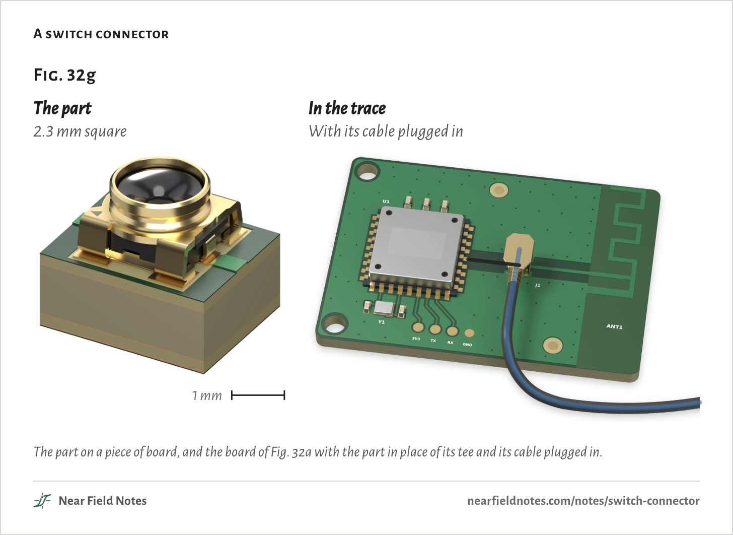
A switch connector goes in the trace where the tee was. It is 2.3 mm square and 1.35 mm tall, and it sits on two signal pads: one toward the radio and one toward the PCB antenna.
With nothing plugged in, the two pads are joined inside the part and the signal passes straight through to the PCB antenna. Push its plug in, and the radio feeds the cable while the PCB antenna is cut off.
These parts were made for factory testing. A probe pressed into one takes the radio’s output and disconnects the antenna, so the radio can be measured alone. I-PEX calls its part the MHF-SW23, Hirose the MS-156C and Murata the SWF.
A switch connector
The part on a piece of board, and the board of Fig. 32a with the part in place of its tee and its cable plugged in.
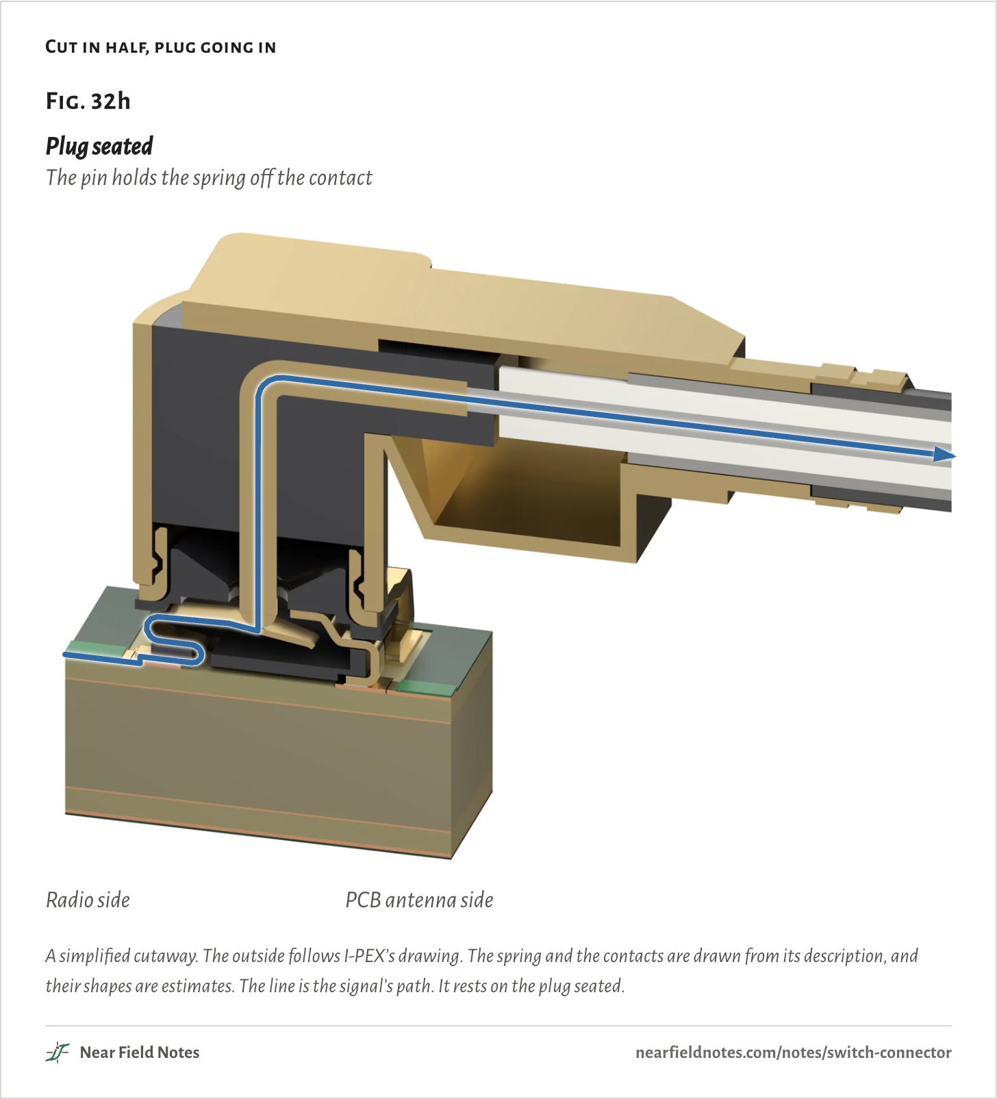
Inside is a spring, fixed at the radio’s end. Its free end presses up against a fixed contact on the antenna’s side.
The plug’s center pin comes down on the spring and pushes it off the contact. The radio now feeds the pin and the cable, and the fixed contact is left alone with the PCB antenna.
So the part has a direction. The spring’s end goes to the radio. Mounted backward, the plug would connect the cable to the PCB antenna and cut the radio off.
Cut in half, plug going in
A simplified cutaway. The outside follows I-PEX’s drawing. The spring and the contacts are drawn from its description, and their shapes are estimates. The line is the signal’s path. It rests on the plug seated.
What the maker guarantees
Fig. 32i
Limit
As I-PEX states it
As power
Cable out, loss through the switch
0.15 dB at most, to 2.5 GHz
96.6% passes
0.20 dB at most, to 6 GHz
95.5% passes
0.40 dB at most, to 11 GHz
91.2% passes
Cable in, isolation to the PCB antenna
20 dB at least, to 3 GHz
1.0% leaks
15 dB at least, to 6 GHz
3.2% leaks
12 dB at least, to 11 GHz
6.3% leaks
Cable in, the plug’s VSWR
1.4 at most, to 3 GHz
2.8% bounces back
1.6 at most, to 6 GHz
5.3% bounces back
2.0 at most, to 9 GHz
11.1% bounces back
Plug-ins
100 for the switch, 30 for the plug
I-PEX’s limits for the MHF-SW23 and its plug harness. As power: the share a loss in dB still passes, the share an isolation in dB lets leak, and the share a VSWR reflects.
594
Switch connector
About 96% to the cable
Field marks. Cable out, the switch passes at least 96.6% to the PCB antenna up to 2.5 GHz. Cable in, at most 1% leaks to the PCB antenna up to 3 GHz and the plug reflects at most 2.8%. Take off 0.2% more for a 100 mΩ contact, and about 96% is left for the cable.
Look-alike. A U.FL. Both are small square parts with a round shell on top, and people call this one a flow-through U.FL. A U.FL has no switch inside, and its plug doesn’t fit this part.
Range. Hirose’s typical curve for its MS-156C with the plug in reads 0.15 to 0.2 dB, so 95.5% to 96.6% passes. Its guaranteed limit is 0.5 dB to 3 GHz, or 89%. To 6 GHz I-PEX’s limits loosen: 95.5% passes with the cable out, and up to 3.2% leaks with it in.
Habitat. Wi-Fi and cellular boards that ship with a PCB antenna and offer an external one. Also test points: Nordic’s development kits put a Murata SWF in the antenna trace to measure the radio.
595
Two other ways
A resistor, or a chip
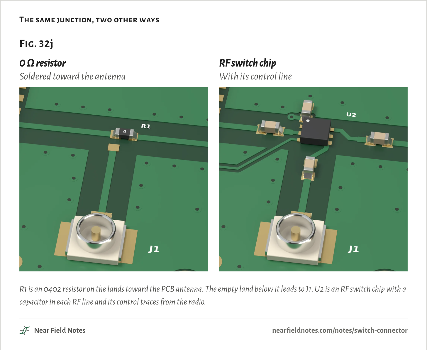
A 0 Ω resistor picks the antenna with solder. The junction gets lands in both directions, and the resistor goes on the pair that leads to the antenna in use. Simulated toward the PCB antenna, 98.0% arrives, against 98.1% for a plain trace.
It is cheap and it loses almost nothing. Changing antennas takes a soldering iron.
An RF switch chip picks the antenna in firmware. A control pin chooses, even while the radio runs, so a product can try both and keep the better one. The chip needs power, a control line and a few capacitors, and a typical one loses 0.45 dB, about 10% of the power.
The same junction, two other ways
R1 is an 0402 resistor on the lands toward the PCB antenna. The empty land below it leads to J1. U2 is an RF switch chip with a capacitor in each RF line and its control traces from the radio.
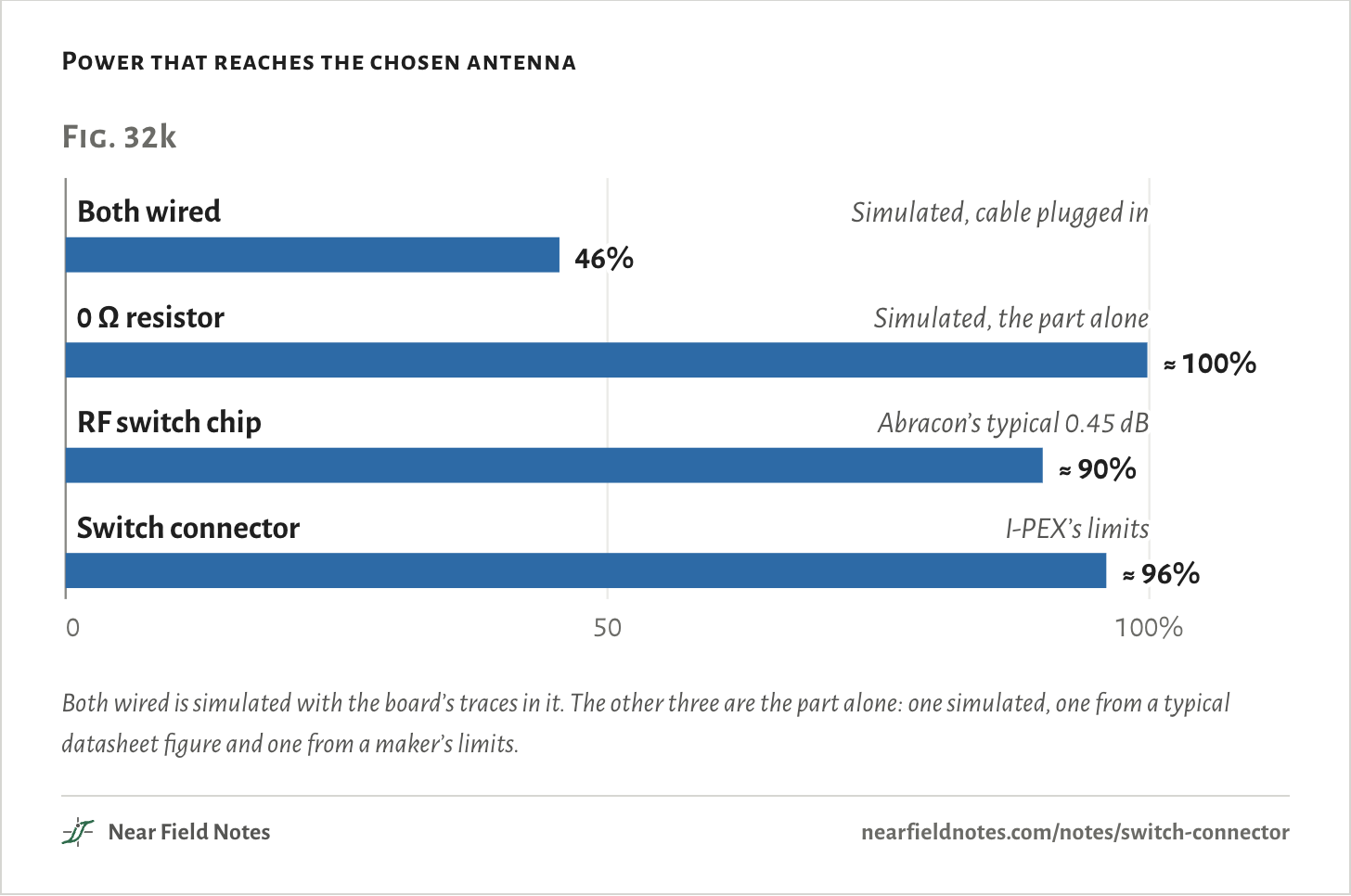
Side by side, only the tee loses half. The other three are within ten points of each other, so the choice comes down to who changes the antenna, and how.
The resistor is set once at the factory. The chip is set by firmware. The switch connector is set by whoever plugs in the cable, and it needs no firmware and no solder.
Its catch is wear. The plug is rated for 30 plug-ins and the switch for 100.
Power that reaches the chosen antenna
Both wired is simulated with the board’s traces in it. The other three are the part alone: one simulated, one from a typical datasheet figure and one from a maker’s limits.The numbers
Way
Reaches the antenna
From
Both wired
45.6%
openEMS, cable plugged in, 2.45 GHz. Includes the board’s traces
0 Ω resistor
99.8%
openEMS: 97.95% with the resistor against 98.13% for a plain trace
RF switch chip
90.2%
Abracon ASWD-S2-0008, 0.45 dB typical and 0.65 dB at most, 2.4 to 2.5 GHz
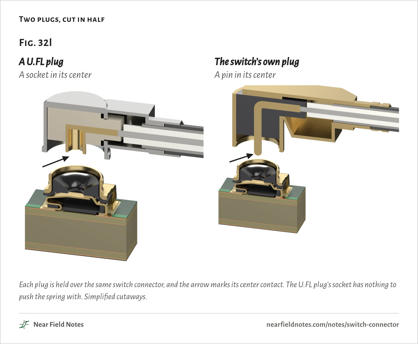
A U.FL cable doesn’t fit a switch connector. A U.FL plug has a socket in its center, because the pin is in the U.FL connector on the board. A switch connector has no pin. Its plug has to bring one, to push the spring.
So the cable is the one made for the switch. I-PEX sells a plug on 1.13 mm coax for the MHF-SW23, part 20851, and lists it for antenna connection. Hirose sells the MS-156C-LP-068 for its MS-156C. Both are rated for 30 plug-ins, the same as a U.FL.
Murata’s SWF and SWG take only Murata’s test probes, so they serve as test points and can’t hold an antenna cable.
Hirose’s sheet also says the MS-156C is for testing a circuit only and cannot be used as an interface, on the same sheet that lists its antenna plug. Ask Hirose before making one a product’s antenna port.
Two plugs, cut in half
Each plug is held over the same switch connector, and the arrow marks its center contact. The U.FL plug’s socket has nothing to push the spring with. Simplified cutaways.
Choosing a way
Who changes the antenna
Any of the three keeps nearly all of the power. What separates them is when the antenna gets chosen.
Key to antenna selection
Resistor, chip or switch connector?
1aThe antenna is chosen once, at the factory0 Ω resistor
1bIt can change after the board shipsGo to 2
2aFirmware chooses, or it changes while the radio runsRF switch chip
2bPlugging in a cable choosesSwitch connector
The board in Fig. 32a ends at 2b. Left as a tee, it gives up half its power with the cable in, and with the cable out its empty branch takes 5.5 GHz away.
Size the branch yourself
Cable out, 0 to 25 mm
Set the length of the empty branch. The line is the share of the radio’s power that reaches the PCB antenna at each frequency, with the cable out.
The notch sits where the branch and its pad add up to a quarter of a wavelength. A longer branch brings it down in frequency, and from 17 mm a second notch comes into view.
Reaches the PCB antenna, against frequency
6 mm of branch: 83% at 2.4 GHz, 0.5% at 5.5 GHz
This branch
No branch
At 2.45 GHz
83%
At 5.5 GHz
0.5%
First notch
5.63 GHz
Each length is its own openEMS run, from 0.5 to 7 GHz. The circles are 2.45 and 5.5 GHz. The first notch is the lowest frequency where less than 10% arrives.The numbers
Cable out. Share of the radio’s power that reaches the PCB antenna.
Branch
At 2.45 GHz
At 5.5 GHz
First notch
0 mm
98%
96%
None
2 mm
95%
80%
Above 7 GHz
4 mm
91%
46%
Above 7 GHz
6 mm
83%
0.5%
5.63 GHz
8 mm
71%
36%
4.42 GHz
10 mm
54%
76%
3.64 GHz
12 mm
30%
91%
3.10 GHz
15 mm
1.0%
91%
2.53 GHz
20 mm
41%
21%
1.94 GHz
25 mm
82%
71%
1.57 GHz
Conditions
Board
34 × 24 mm, 1.6 mm thick, 4 layers. JLCPCB’s JLC04161H-7628 stack: 0.2104 mm of 7628 prepreg under the top layer, permittivity 4.4, loss tangent 0.018.
Traces
50 Ω microstrip, 0.373 mm wide: 49.4 Ω and an effective permittivity of 3.23 in the solve. Radio to the junction 5.5 mm, junction to the PCB antenna 7.5 mm, junction to J1’s pad 6 mm. The pad is 1.0 × 1.0 mm.
Solver
openEMS, a 3D field solver, 117 runs. Cells are 0.025 mm at copper edges and 0.1 mm along the traces, with 4 through the prepreg.
Ends
The radio, the PCB antenna and the cable are each a matched 50 Ω port. Copper is a perfect conductor, so the board’s loss is its FR-4’s: 0.063 dB/cm at 2.45 GHz and 0.142 dB/cm at 5.5 GHz.
Connector
Only J1’s signal pad is in the model, without the connector’s body or its center contact. The cable is a 50 Ω port at the pad, and its own loss is left out.
Shares
Of the power the radio sends into its trace. On this page 2.4 GHz means 2.45 GHz, the band’s middle.
Switch connector
Not simulated. I-PEX’s limits for the MHF-SW23 to 3 GHz, as power: a plug VSWR of 1.4, 20 dB of isolation and a 100 mΩ contact.
RF switch chip
Not simulated. Abracon’s ASWD-S2-0008, 0.45 dB typical from 2.4 to 2.5 GHz.
0 Ω resistor
Simulated as a metal bridge the size of an 0402 on its lands. The part alone passes 99.8%: its run against the plain trace’s.
Checks
A finer mesh moves no share by more than 0.15 points. With a 50 Ω line past the pad in place of the cable’s port, the tee gives 45.2%, 40.0% and 13.5%.
Renders
Blender. The switch connector’s outside is from I-PEX’s drawing. Its inside is estimated.
Simulated only. Nothing on this page has been measured on a board yet.
Limits
Real antennas aren’t 50 Ω across a band, and the split moves with them.
With both wired, both antennas radiate at once. How the two add up in the air isn’t simulated.
Real copper adds about 0.05 dB/cm at 2.45 GHz, as Note 25 found. On this board that is about half a point.
A real U.FL connector adds a little more capacitance than its pad alone, so the dips would come at slightly shorter branches.
The switch connector’s 96% is the part alone, built from limits. This board’s 5.5 mm of trace ahead of it would take 0.8% more.
The limits are I-PEX’s, for one part. Other makers’ parts have their own.
Files
layout.pyThe board: its stack, its traces and the four things that can sit at the junction
sim/tee.pyThe openEMS model of the tee, the empty branch and the 0 Ω resistor
sim/batch.pyEvery run on this page: the main cases, the 43 branch lengths and the checks
sim/post.pyEach run’s shares of power, and the sweeps against length and frequency
sim/theory.pyThe transmission-line sums the runs are checked against
render/board.pyThe board and its junction, four ways
render/connector.pyThe switch connector, its plug and the cutaways