Near Field Notes

Note 36PowerRev 1Watch the video · 1:56

Power inductors, part 2

Is a toroid the quietest inductor?

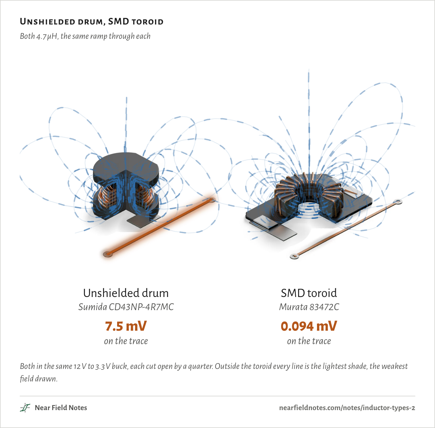
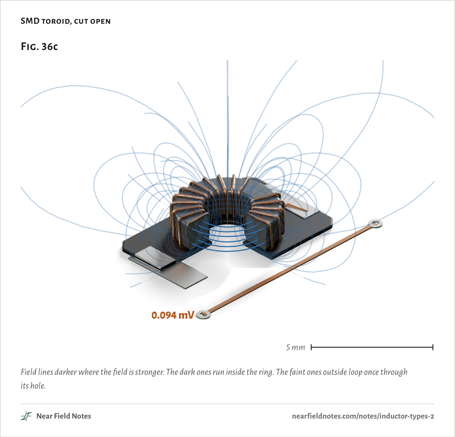
Almost. A 4.7 µH SMD toroid puts 0.094 mV on a trace 1 mm away, where an unshielded drum puts 7.5 mV, 80 times as much. Only a pot core with its gap in the center post puts less, 0.036 mV.

A toroid’s wire wraps all the way around its ring, so the ring carries the field in a closed loop. What leaks is one turn’s worth.

The figure runs the same current ramp through both parts. The lines are the field, darker where it is stronger, and each trace glows with the voltage it picks up.

Unshielded drum, SMD toroid

Both 4.7 µH, the same ramp through each

Unshielded drumSumida CD43NP-4R7MC7.5 mVon the traceSMD toroidMurata 83472C0.094 mVon the traceUnshielded drumSumida CD43NP-4R7MC7.5 mVon the traceSMD toroidMurata 83472C0.094 mVon the traceUnshielded drumSumida CD43NP-4R7MC7.5 mVon the traceSMD toroidMurata 83472C0.094 mVon the trace
Both in the same 12 V to 3.3 V buck, each cut open by a quarter. Outside the toroid every line is the lightest shade, the weakest field drawn.

Six more ways to build an inductor

Cut open, at true size

Note 12 compared five common ways to build a 4.7 µH power inductor.

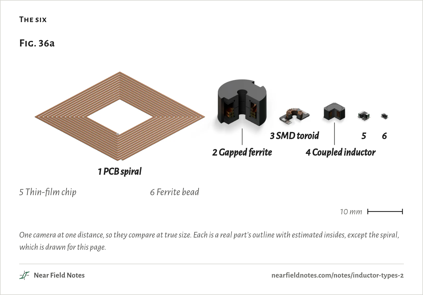
These are six more. Four can take the place of those five in a buck: a toroid, a gapped ferrite pot core, a thin-film chip and a spiral printed in the board’s copper.

The other two do different jobs. A coupled inductor puts two windings on one core, and a ferrite bead filters noise.

The six
Fig. 36a1 PCB spiral2 Gapped ferrite563 SMD toroid4 Coupled inductor5 Thin-film chip6 Ferrite bead10 mmFig. 36a1 PCB spiral3 SMD toroid562 Gapped ferrite4 Coupled inductor5 Thin-film chip6 Ferrite bead10 mmFig. 36a1 PCB spiral3 SMD toroid562 Gapped ferrite4 Coupled inductor5 Thin-film chip6 Ferrite bead10 mm
One camera at one distance, so they compare at true size. Each is a real part’s outline with estimated insides, except the spiral, which is drawn for this page.

The noise test is the one from Note 12.

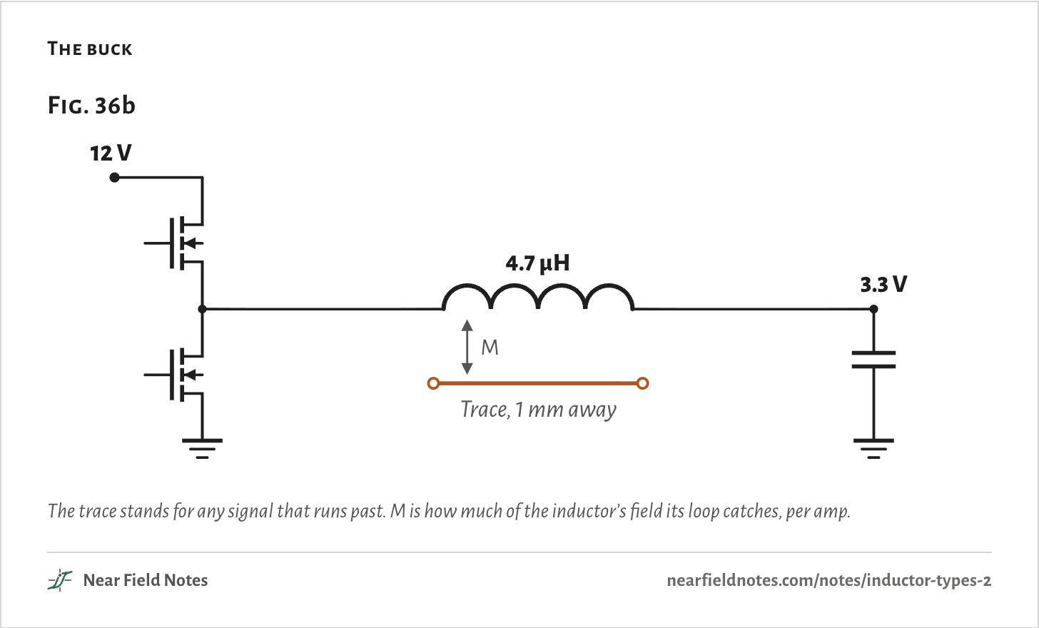
A 12 V to 3.3 V buck ramps the inductor’s current 1.85 A every µs while its top switch is on. A trace 10 mm long runs past, 1 mm from the part’s body, with its return in the ground plane 0.2 mm below.

The voltage on that trace is the mutual inductance M times the ramp. The coupled inductor and the bead do other jobs, so they sit out the test.

The buck
Fig. 36b12 V4.7 µH3.3 VTrace, 1 mm awayMFig. 36b12 V4.7 µH3.3 VTrace, 1 mm awayMFig. 36b12 V4.7 µH3.3 VTrace, 1 mm awayM
The trace stands for any signal that runs past. M is how much of the inductor’s field its loop catches, per amp.

SMD toroid

Murata 83472C

A toroid’s wire passes through a ring and back around it, turn after turn, all the way round. Its field runs around inside the ring, which has no ends for it to leave by.

SMD toroid, cut open
Fig. 36c0.094 mV5 mmFig. 36c0.094 mV5 mmFig. 36c0.094 mV5 mm
Field lines darker where the field is stronger. The dark ones run inside the ring. The faint ones outside loop once through its hole.
612

The one turn that leaks

Where the return wire runs

Zhang and Wang split a toroid’s field in two. The turns, spread evenly around the ring, keep nearly all of theirs inside the core. But as it winds, the wire also advances once around the ring, and that one trip acts like a single turn the size of the toroid.

So one turn of the toroid leaks, where the unshielded drum leaks from all 17 of its turns.

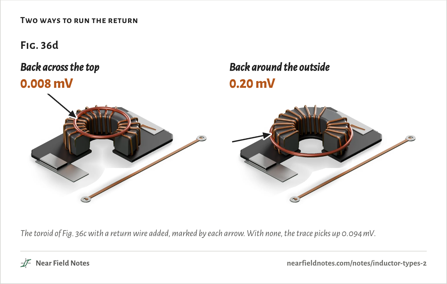
A wire run back the other way can cancel that turn. Run back across the top, along the middle of the winding, it brings the trace down to 0.008 mV. Run around the outside of the ring, it doubles the voltage, to 0.20 mV.

The top return runs at the ring’s mean radius, 1.68 mm from the center, close to the 1.76 mm of the advancing turn as modeled. The outside return runs at 2.46 mm, beyond the ring.

Two ways to run the return
Fig. 36dBack across the top0.008 mVBack around the outside0.20 mVFig. 36dBack across the top0.008 mVBack around the outside0.20 mVFig. 36dBack across the top0.008 mVBack around the outside0.20 mV
The toroid of Fig. 36c with a return wire added, marked by each arrow. With none, the trace picks up 0.094 mV.
The numbers
The same 4.7 µH toroid model, 1 A through it.
Return wireM to the traceOn the trace
No return wire0.0507 nH0.094 mV
Back across the top, at the ring’s mean radius0.0044 nH0.008 mV
Back around the outside of the ring0.1069 nH0.20 mV

Gapped ferrite

TDK P 14x8 pot core

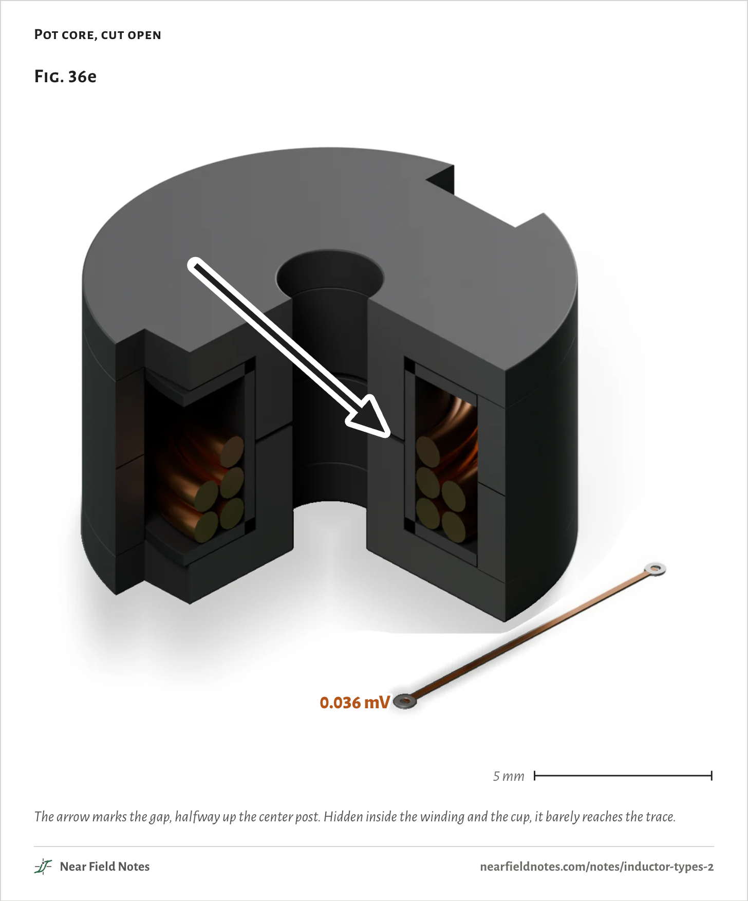
A gapped ferrite inductor winds its wire on a former between two halves of ferrite. A thin air gap between them holds most of the stored energy and sets the inductance.

Pot core, cut open
Fig. 36e0.036 mV5 mmFig. 36e0.036 mV5 mmFig. 36e0.036 mV5 mm
The arrow marks the gap, halfway up the center post. Hidden inside the winding and the cup, it barely reaches the trace.
614

Where the gap sits

In the post, or as a spacer

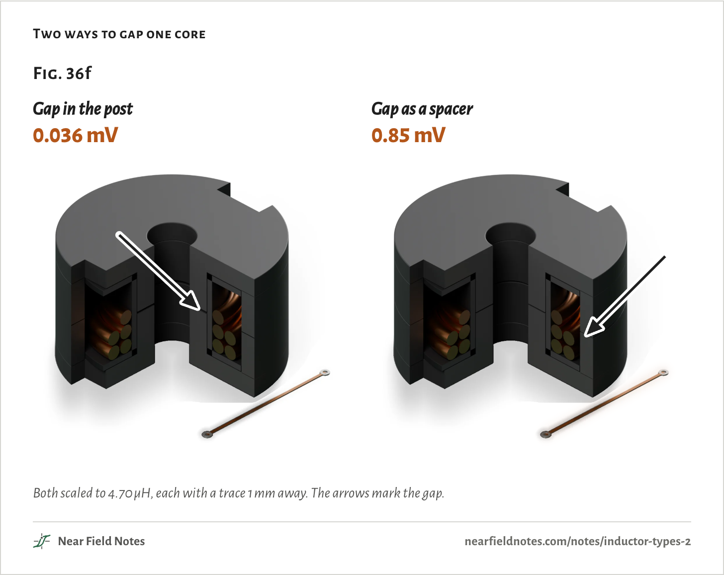
The gap can go in two places. Cut into the center post, it sits inside the winding and the cup. Made by holding the two halves apart with a spacer, half of it ends up in the outer wall.

The outer wall faces the board. The same core with a spacer gap puts 0.85 mV on the trace, 24 times as much as with the gap in the post.

TI’s magnetics design notes warn of it: spacing the halves apart “propagates considerable stray flux outside the inductor”.

Two ways to gap one core
Fig. 36fGap in the post0.036 mVGap as a spacer0.85 mVFig. 36fGap in the post0.036 mVGap as a spacer0.85 mVFig. 36fGap in the post0.036 mVGap as a spacer0.85 mV
Both scaled to 4.70 µH, each with a trace 1 mm away. The arrows mark the gap.
The numbers
Ferrite µ 2300 unless stated. Each run’s M is scaled to 4.70 µH by M ∝ √L.
GapModelM as runM at 4.70 µHOn the trace
Gap in the post4.99 µH0.0200 nH0.0194 nH0.036 mV
Gap as a spacer4.79 µH0.4640 nH0.4595 nH0.85 mV
Gap in the post, ferrite µ 10004.70 µH0.080 mV
Gap in the post, ferrite µ 5004.75 µH0.15 mV
Gap as a spacer, ferrite µ 10004.70 µH0.87 mV

The gap heats the wire

A second build, seven turns at 500 kHz

This section uses a second build of the same P 14x8 pot core: M33 ferrite, permeability 750, with a 0.30 mm gap in the post. The noise test above used N48 with a 0.16 mm gap. Seven turns of 0.65 mm wire carry 1 A peak at 500 kHz.

The gap’s field bulges out into the winding beside it and drives eddy currents in the wire. TI’s notes say windings near a gap “have been known to melt”.

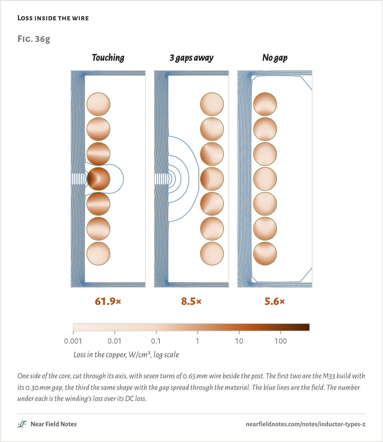
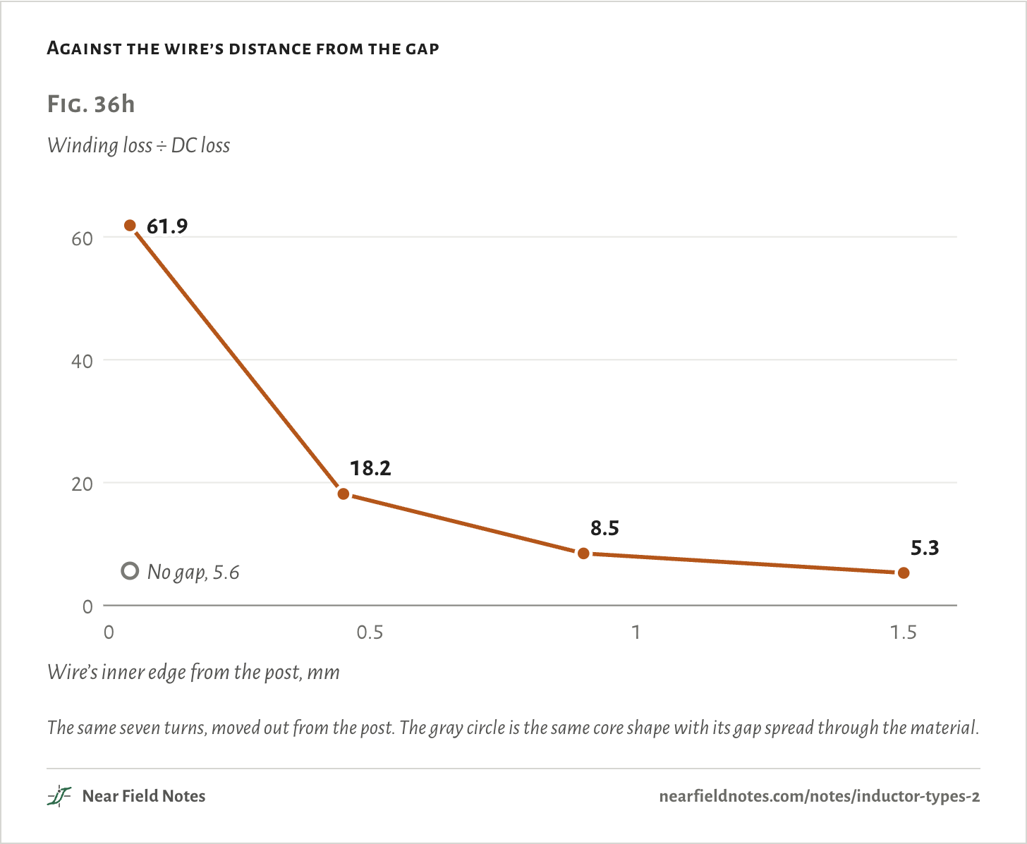
With the wire wound against the post, this build’s winding loses 61.9 times its DC loss. The turn beside the gap takes 72% of it.

The same core shape with its gap spread through the material, a permeability of 64 throughout, loses 5.6 times its DC loss.

Loss inside the wire
Fig. 36gTouching61.9×3 gaps away8.5×No gap5.6×0.0010.110100Loss in the copper, W/cm³, log scaleFig. 36gTouching61.9×3 gaps away8.5×No gap5.6×0.0010.010.1110100Loss in the copper, W/cm³, log scaleFig. 36gTouching61.9×3 gaps away8.5×No gap5.6×0.0010.010.1110100Loss in the copper, W/cm³, log scale
One side of the core, cut through its axis, with seven turns of 0.65 mm wire beside the post. The first two are the M33 build with its 0.30 mm gap, the third the same shape with the gap spread through the material. The blue lines are the field. The number under each is the winding’s loss over its DC loss.

Moving the wire out helps. Severns’ rule of thumb keeps it two to three gap lengths from the gap.

This build’s gap is 0.30 mm. On TDK’s coil former, 0.45 mm out, the loss falls to 18.2 times, and three gap lengths out, to 8.5 times. That is still more than with no gap, 5.6 times with the wire touching.

Magnetics notes that powder cores, whose gap is spread through the material, “are not susceptible to fringing losses”.

Against the wire’s distance from the gap
Fig. 36hWinding loss ÷ DC loss020406000.511.5Wire’s inner edge from the post, mm61.918.28.55.3No gap, 5.6Fig. 36hWinding loss ÷ DC loss020406000.511.5Wire’s inner edge from the post, mm61.918.28.55.3No gap, 5.6Fig. 36hWinding loss ÷ DC loss020406000.511.5Wire’s inner edge from the post, mm61.918.28.55.3No gap, 5.6
The same seven turns, moved out from the post. The gray circle is the same core shape with its gap spread through the material.
The numbers
Seven turns of 0.65 mm wire, 1 A peak in each, 500 kHz. The DC resistance rises as the wire moves out, since each turn gets longer.
Wire’s inner edge from the postGapDC resistanceAt 500 kHzRatio
0.05 mm0.30 mm7.60 mΩ470.1 mΩ61.9
0.45 mm, on TDK’s coil former0.30 mm8.51 mΩ154.6 mΩ18.2
0.9 mm0.30 mm9.54 mΩ80.7 mΩ8.5
1.5 mm0.30 mm10.91 mΩ57.9 mΩ5.3
0.05 mmNone, µ 64 core7.60 mΩ42.8 mΩ5.6

Coupled inductor

Coilcraft LPD5030-472

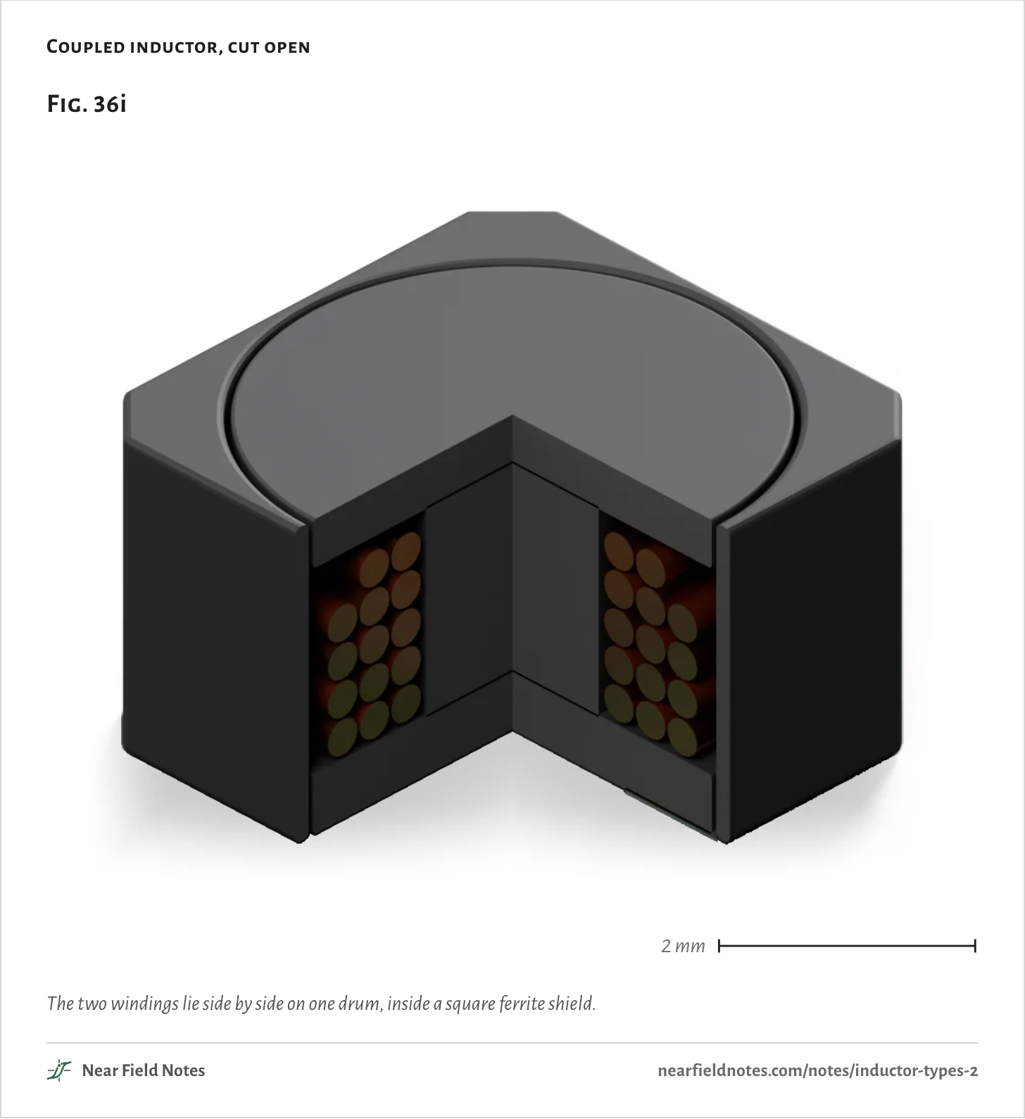
A coupled inductor winds two windings together on one core, so current in either one sets up field through both.

Coupled inductor, cut open
Fig. 36i2 mmFig. 36i2 mmFig. 36i2 mm
The two windings lie side by side on one drum, inside a square ferrite shield.
616

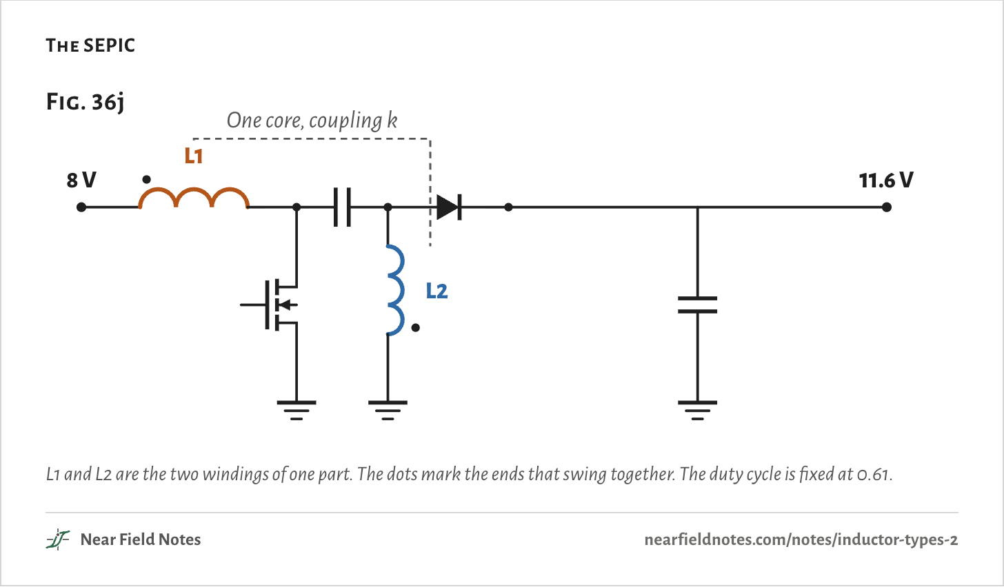
A SEPIC makes an output above or below its input with two inductors. Both see the same voltage at every instant, so one coupled part can do the job of the pair.

This one runs from 8 V to 11.6 V at about 1 A, switching at 500 kHz. With two separate 4.7 µH inductors, each one’s current ripples 2.0 A peak to peak. Wound on one core at k 0.90, each ripples 1.1 A, close to the 1.0 A of two separate 9.4 µH parts.

TI gives the rule: coupled, a SEPIC needs only half the inductance, because the mutual inductance splits the ripple equally between the windings.

The SEPIC
Fig. 36j8 VL1L211.6 VOne core, coupling kFig. 36j8 VL1L211.6 VOne core, coupling kFig. 36j8 VL1L211.6 VOne core, coupling k
L1 and L2 are the two windings of one part. The dots mark the ends that swing together. The duty cycle is fixed at 0.61.

Couple the windings yourself

Separate, to k 0.999

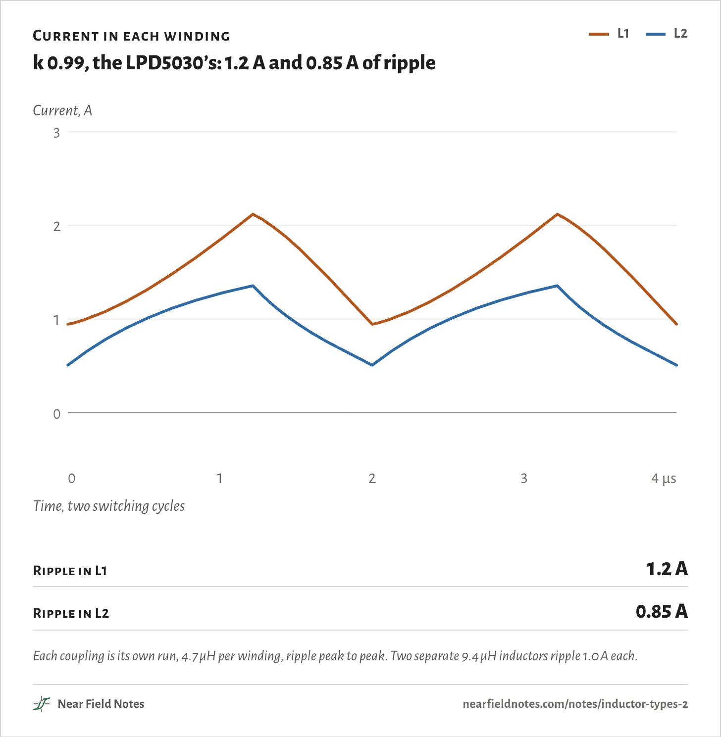
Set how tightly the two windings couple. The lines are each winding’s current over two switching cycles of the SEPIC.

Up to about 0.95 the ripple splits evenly. Tighter than that it moves into L1. At the LPD5030’s 0.99 the windings ripple 1.2 A and 0.85 A. TI advises 10 to 15% leakage for a SEPIC.

k = 0.99
Current in each winding

k 0.99, the LPD5030’s: 1.2 A and 0.85 A of ripple

  • L1
  • L2
Current, A012301234 µsTime, two switching cyclesCurrent, A012301234 µsTime, two switching cyclesCurrent, A012301234 µsTime, two switching cycles
Ripple in L1
1.2 A
Ripple in L2
0.85 A
Each coupling is its own run, 4.7 µH per winding, ripple peak to peak. Two separate 9.4 µH inductors ripple 1.0 A each.
The numbers
Peak to peak, 4.7 µH per winding unless stated.
CouplingRipple in L1Ripple in L2
Separate2.0 A2.0 A
k = 0.901.1 A1.1 A
k = 0.951.0 A1.0 A
k = 0.981.1 A0.97 A
k = 0.991.2 A0.85 A
k = 0.9951.3 A0.68 A
k = 0.9991.5 A0.51 A
Two separate 9.4 µH1.0 A1.0 A

Thin-film chip

TDK TFM252012ALMA4R7MTAA

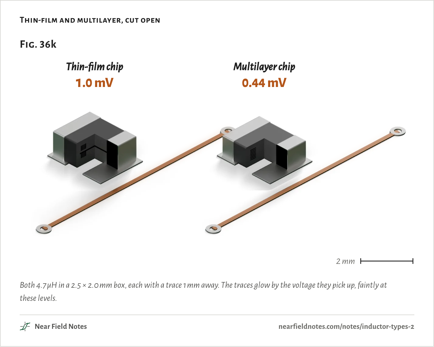
A thin-film chip forms its coil as a film of copper and buries it in metal powder bound in resin, in the same small box as a multilayer chip.

Thin-film and multilayer, cut open
Fig. 36kThin-film chip1.0 mVMultilayer chip0.44 mV2 mmFig. 36kThin-film chip1.0 mVMultilayer chip0.44 mV2 mmFig. 36kThin-film chip1.0 mVMultilayer chip0.44 mV2 mm
Both 4.7 µH in a 2.5 × 2.0 mm box, each with a trace 1 mm away. The traces glow by the voltage they pick up, faintly at these levels.
618

Thin-film against multilayer

From each datasheet

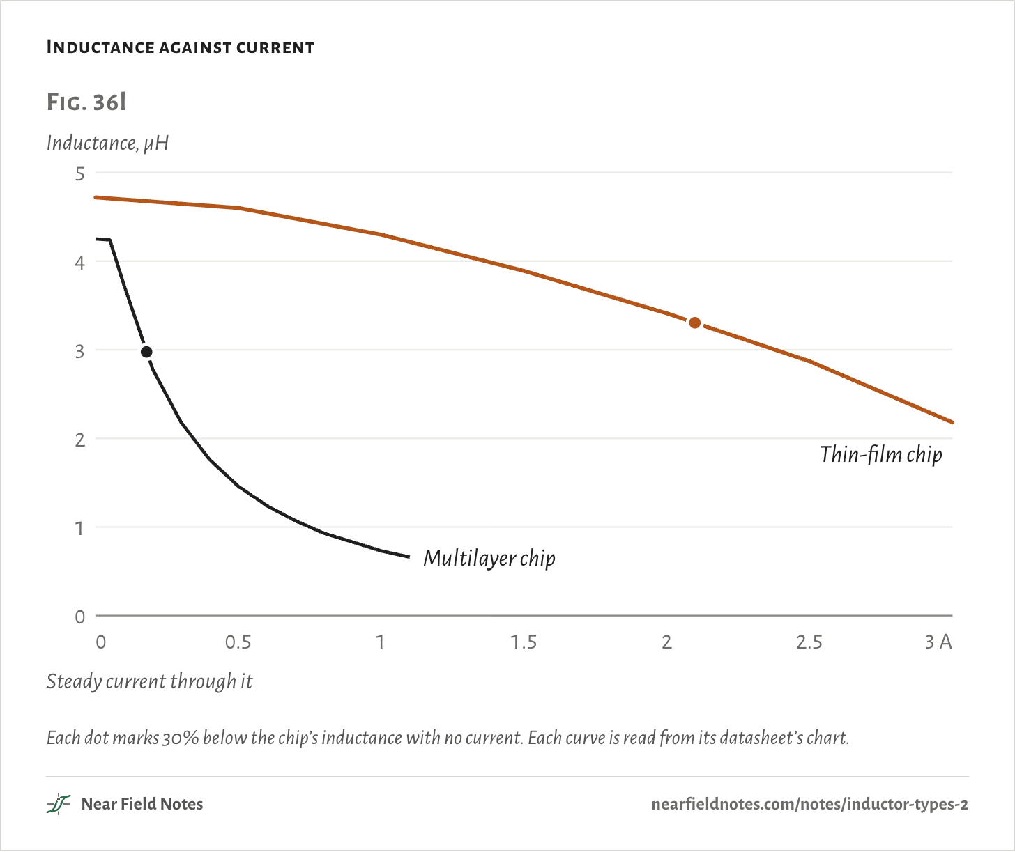
Both are sold as 4.7 µH. As the current rises, the multilayer chip’s ferrite gives way almost at once. The thin-film chip’s metal powder holds on, which TDK’s patent credits to metal’s better behavior under DC.

The thin-film chip carries 12 times the current to the same 30% drop. In return it puts 2.3 times the voltage on the trace, and its winding is 180 mΩ against 110 mΩ typical.

Inductance against current
Fig. 36lInductance, µH0123450123 ASteady current through itThin-film chipMultilayer chipFig. 36lInductance, µH01234500.511.522.53 ASteady current through itThin-film chipMultilayer chipFig. 36lInductance, µH01234500.511.522.53 ASteady current through itThin-film chipMultilayer chip
Each dot marks 30% below the chip’s inductance with no current. Each curve is read from its datasheet’s chart.
The numbers
Read from TDK’s chart, and from Murata’s at 20 °C as in Note 12. 30% down at 2.1 A and 0.18 A.
CurrentThin-film chipMultilayer chip
0 A4.72 µH4.25 µH
0.05 A4.24 µH
0.1 A3.73 µH
0.2 A2.78 µH
0.3 A2.18 µH
0.4 A1.76 µH
0.5 A4.60 µH1.46 µH
0.6 A1.24 µH
0.7 A1.07 µH
0.8 A0.93 µH
0.9 A0.83 µH
1 A4.30 µH0.73 µH
1.1 A0.66 µH
1.5 A3.89 µH
2 A3.41 µH
2.5 A2.87 µH
3 A2.18 µH

Ferrite bead

Würth 74279228111

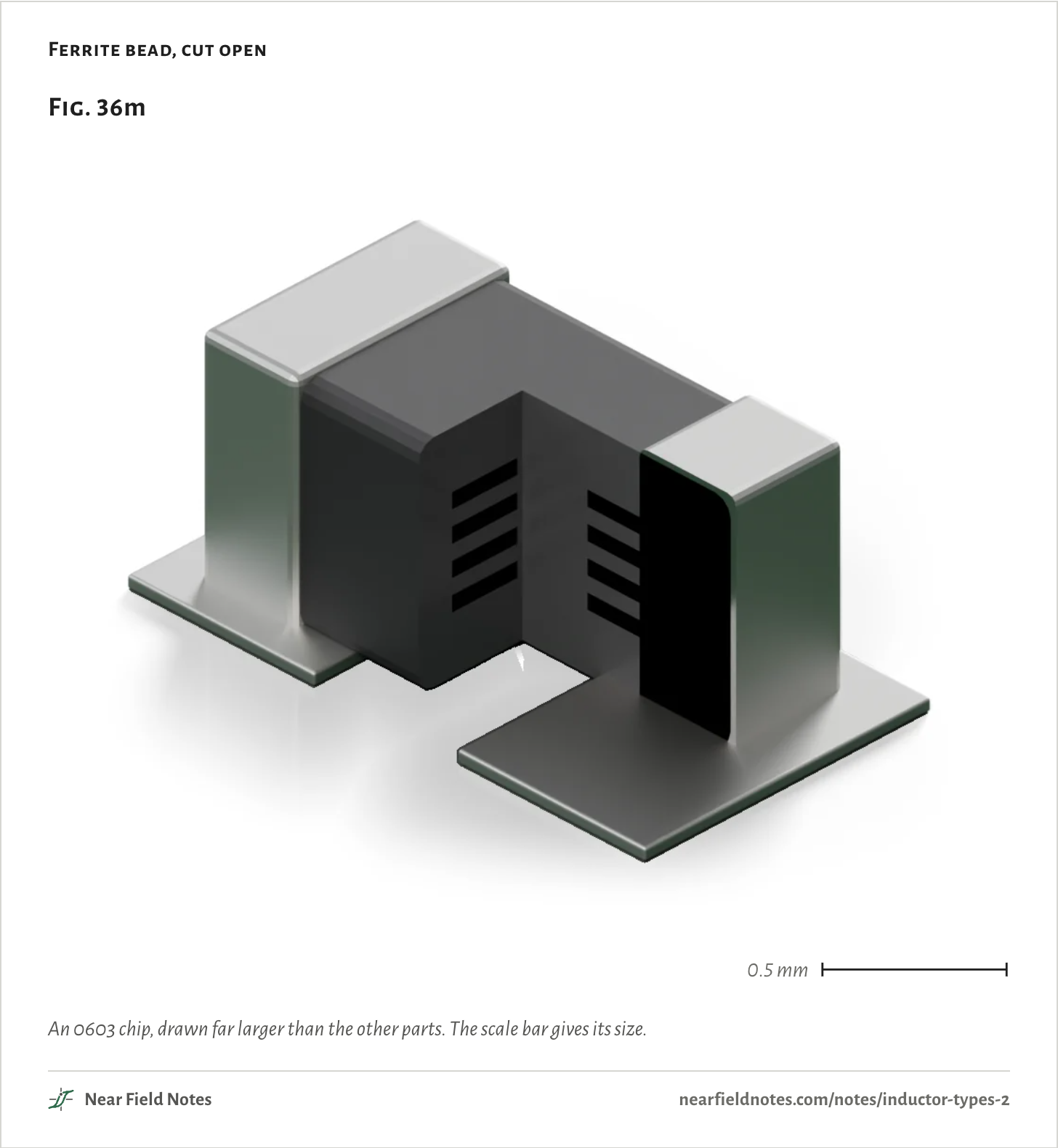
A ferrite bead is a few turns of conductor inside a lossy ferrite. Above a certain frequency it acts as a resistor and turns noise into heat.

Ferrite bead, cut open
Fig. 36m0.5 mmFig. 36m0.5 mmFig. 36m0.5 mm
An 0603 chip, drawn far larger than the other parts. The scale bar gives its size.
620

A bead under DC

Impedance at 100 MHz

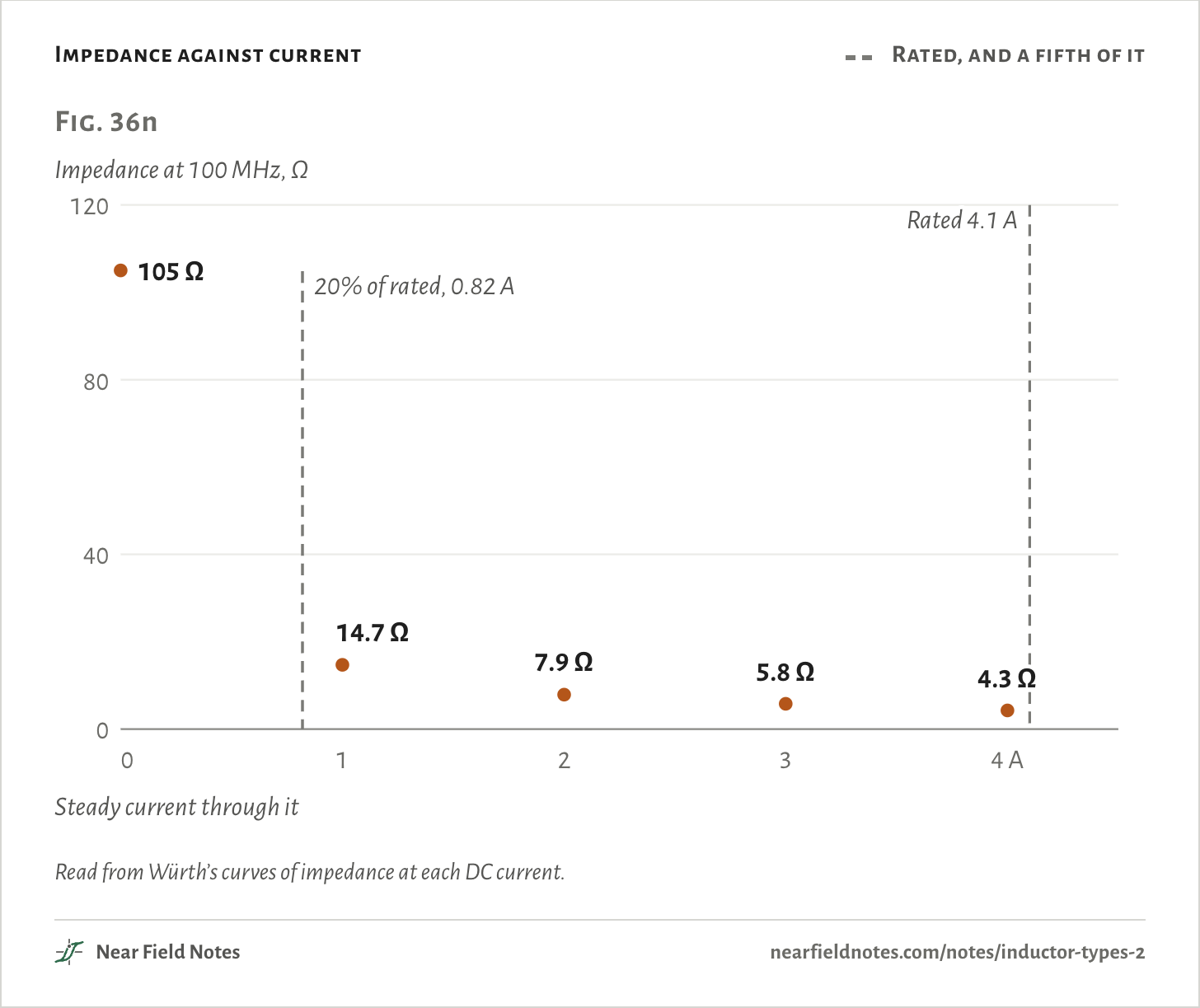
A bead’s headline impedance is measured with no current through it. Run the load’s DC through it and its ferrite saturates.

This one has lost 86% of its impedance at 100 MHz by 1 A, a quarter of its rating. The 4.1 A rating is a heating limit.

With a ceramic capacitor after it, a bead can also ring. Analog Devices measured a bead and a 10 nF capacitor adding 10 dB at 2.4 MHz, the frequency they were there to filter.

Impedance against current
  • Rated, and a fifth of it
Fig. 36nImpedance at 100 MHz, Ω0408012001234 ASteady current through itRated 4.1 A20% of rated, 0.82 A105 Ω14.7 Ω7.9 Ω5.8 Ω4.3 ΩFig. 36nImpedance at 100 MHz, Ω0408012001234 ASteady current through itRated 4.1 A20% of rated, 0.82 A105 Ω14.7 Ω7.9 Ω5.8 Ω4.3 ΩFig. 36nImpedance at 100 MHz, Ω0408012001234 ASteady current through itRated 4.1 A20% of rated, 0.82 A105 Ω14.7 Ω7.9 Ω5.8 Ω4.3 Ω
Read from Würth’s curves of impedance at each DC current.
The numbers
Read by eye from Würth’s DC-bias curves, about ±10%.
CurrentAt 100 MHzLost
0 A105 Ω
1 A14.7 Ω86%
2 A7.9 Ω92%
3 A5.8 Ω94%
4 A4.3 Ω96%

PCB spiral

12 turns, 35 mm square

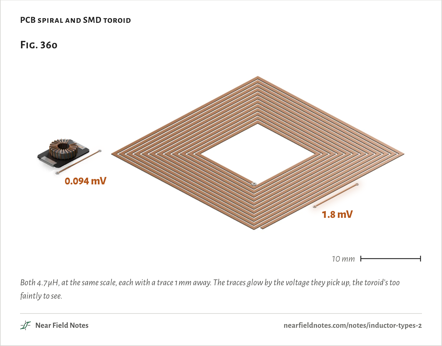
A PCB spiral is a trace wound into a flat coil on one layer, its inner end brought out through a via. It has no core at all.

PCB spiral and SMD toroid
Fig. 36o1.8 mV0.094 mV10 mmFig. 36o1.8 mV0.094 mV10 mmFig. 36o1.8 mV0.094 mV10 mm
Both 4.7 µH, at the same scale, each with a trace 1 mm away. The traces glow by the voltage they pick up, the toroid’s too faintly to see.
622

The plane under a spiral

Cut out, or solid

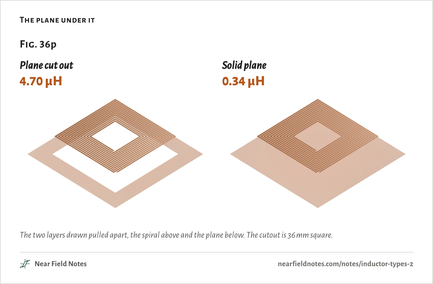
A 4-layer board has a ground plane right under its top layer. With the plane cut away under it, the spiral is 4.70 µH. Over a solid plane 0.2 mm down, the same spiral is 0.34 µH, 93% less.

With no core, it also puts the most on the trace of any part in this note, 1.8 mV. Kamby and colleagues give stray field as their reason for printing a toroid on a board instead of a spiral.

The plane under it
Fig. 36pPlane cut out4.70 µHSolid plane0.34 µHFig. 36pPlane cut out4.70 µHSolid plane0.34 µHFig. 36pPlane cut out4.70 µHSolid plane0.34 µH
The two layers drawn pulled apart, the spiral above and the plane below. The cutout is 36 mm square.
The numbers
The plane is a perfect conductor at the ripple’s frequency in the model.
SpiralTurnsInductance
Plane cut out under it12.324.70 µH
Solid plane 0.2 mm below120.34 µH
Mohan’s formula, no plane124.76 µH

Noise on the trace

Every 4.7 µH part in the test

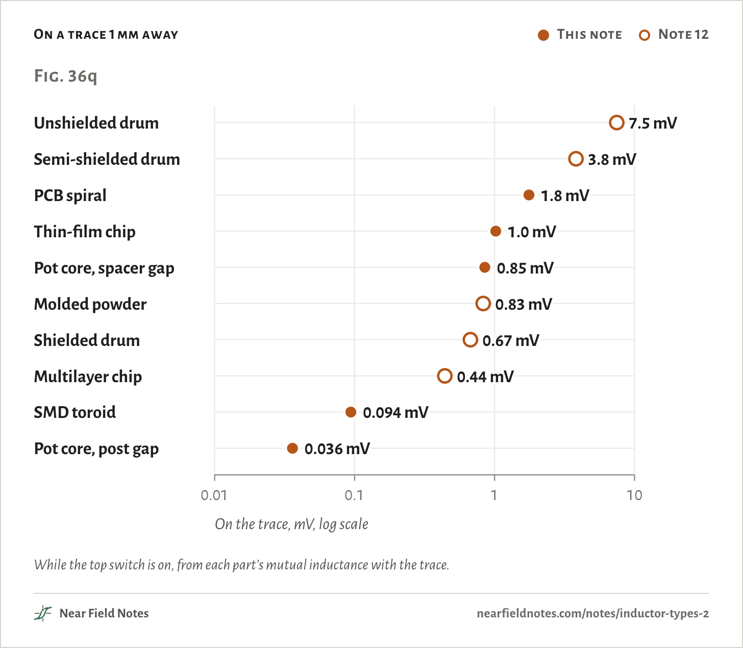
Beside Note 12’s five, the pot core with its gap in the post is the quietest, and the SMD toroid comes next, 80 times below the unshielded drum.

The same pot core with a spacer gap lands beside the molded and shielded parts. The spiral, with no core, puts more on the trace than any other part here except two drums.

On a trace 1 mm away
  • This note
  • Note 12
Fig. 36qUnshielded drum7.5 mVSemi-shielded drum3.8 mVPCB spiral1.8 mVThin-film chip1.0 mVPot core, spacer gap0.85 mVMolded powder0.83 mVShielded drum0.67 mVMultilayer chip0.44 mVSMD toroid0.094 mVPot core, post gap0.036 mV0.010.1110On the trace, mV, log scaleFig. 36qUnshielded drum7.5 mVSemi-shielded drum3.8 mVPCB spiral1.8 mVThin-film chip1.0 mVPot core, spacer gap0.85 mVMolded powder0.83 mVShielded drum0.67 mVMultilayer chip0.44 mVSMD toroid0.094 mVPot core, post gap0.036 mV0.010.1110On the trace, mV, log scaleFig. 36qUnshielded drum7.5 mVSemi-shielded drum3.8 mVPCB spiral1.8 mVThin-film chip1.0 mVPot core, spacer gap0.85 mVMolded powder0.83 mVShielded drum0.67 mVMultilayer chip0.44 mVSMD toroid0.094 mVPot core, post gap0.036 mV0.010.1110On the trace, mV, log scale
While the top switch is on, from each part’s mutual inductance with the trace.
The numbers
While the top switch is on, the current climbs 1.85 A every µs.
BuildPartM to the traceOn the traceFrom
Unshielded drumSumida CD43NP-4R7MC4.0329 nH7.5 mVNote 12
Semi-shielded drumBourns SRN4018BTA-4R7M2.0645 nH3.8 mVNote 12
PCB spiral12 turns, 35 mm square0.9518 nH1.8 mVNote 36
Thin-film chipTDK TFM252012ALMA4R7MTAA0.5509 nH1.0 mVNote 36
Pot core, spacer gapTDK P 14x80.4595 nH0.85 mVNote 36
Molded powderCoilcraft XAL4030-4720.4478 nH0.83 mVNote 12
Shielded drumBourns SRR4018-4R7Y0.3634 nH0.67 mVNote 12
Multilayer chipMurata LQM2HPN4R7MG0L0.2381 nH0.44 mVNote 12
SMD toroidMurata 83472C0.0507 nH0.094 mVNote 36
Pot core, post gapTDK P 14x80.0194 nH0.036 mVNote 36

Which build?

Five questions

The job decides first, then the switching frequency, the space and the inductance.

Key to six inductors

Bead, coupled, spiral, thin-film, gapped ferrite or toroid?

  1. 1aIt filters a supply pin’s noise at tens to hundreds of MHzFerrite bead
  2. 1bIt stores energy in a converterGo to 2
  3. 2aThe converter has two windings to feed, as a SEPIC doesCoupled inductor
  4. 2bIt has oneGo to 3
  5. 3aIt switches at tens of MHz and needs tens of nHPCB spiral
  6. 3bIt switches below a few MHz and needs microhenriesGo to 4
  7. 4aThe board is tight and the current under about 2 AThin-film chip
  8. 4bThere is roomGo to 5
  9. 5aThe inductance must hold to a few percentGapped ferrite, gap in the post
  10. 5b20% will doSMD toroid

Both ends of 5 are quiet: 0.036 mV on the trace with the gap in the post, 0.094 mV for the toroid. For amps in a small space, a molded powder part carries more current than this toroid in a smaller box.

Conditions

Parts
Murata 83472C, TDK P 14x8 pot core B65541, Coilcraft LPD5030-472, TDK TFM252012ALMA4R7MTAA and Würth 74279228111, with outlines from their datasheets. The spiral is a 12-turn square of 0.6 mm trace and 0.3 mm gaps, 35 mm on a side.
Models
Insides estimated. The toroid’s ring has a permeability of 60 and 21.4 turns. The pot core is N48 ferrite, permeability 2300, with a 0.16 mm gap. The thin-film chip’s metal powder has a permeability of 25. Each model’s turns set so it simulates 4.70 µH. The two pot core runs came to 4.99 and 4.79 µH and are scaled to 4.70 µH by M ∝ √L.
Toroid
An evenly wound ring’s turns keep nearly all their field inside it, so only the winding’s one trip around the ring is in the field model, spread over the winding. Its turns’ inductance is calculated.
Board
A ground plane 0.2 mm under the top copper, a perfect conductor at the ripple’s frequency. Under the spiral it has a 36 mm square cutout, except in the solid-plane run.
Trace
10 mm long, 1 mm from the body’s side, centered on the part, its return in the plane, as in Note 12
Buck
12 V to 3.3 V. While the top switch is on, the current climbs 1.85 A every µs.
Gap loss
TDK P 14x8 in M33 ferrite, permeability 750, 100 nH per turn squared with a 0.30 mm gap in the post. Seven turns of 0.65 mm solid copper in one layer, each its own conductor with 1 A peak at 500 kHz. The no-gap core has a permeability of 64 throughout.
SEPIC
8 V in, a fixed duty cycle of 0.61, 500 kHz, a 12 Ω load, giving 11.6 V. A 12 mΩ switch, a Schottky diode, 10 µF of coupling and 44 µF of output capacitance, and 111 mΩ in each winding, the LPD5030-472’s most.
Curves
Read by eye from each datasheet’s chart. The multilayer chip’s is Note 12’s, at 20 °C.
Solvers
Elmer, 3D magnetostatics at 1 A, 13 runs for the trace test. Elmer, 2D axisymmetric at 500 kHz, 6 runs for the gap loss. ngspice, 9 runs for the SEPIC.
Ratio
The toroid’s 80 times is the ratio of the two mutual inductances with the trace, 4.0329 nH for Note 12’s unshielded drum and 0.0507 nH for the toroid, 79.5 unrounded.
Checks
Note 12’s unshielded drum and molded part, rerun here, give 7.454 mV and 0.827 mV against Note 12’s 7.465 mV and 0.829 mV. The gap-loss model at 100 Hz gives 0.9986 times the DC loss.
Renders
Blender, from the same models

Simulated only. Nothing on this page has been measured on a board yet.

Limits

  • The insides are estimates, and real ones will move each number.
  • The toroid’s leads aren’t modeled. Its whole outside field is one turn’s worth, so its leads matter more than a drum’s.
  • The pot core’s leak through its wire slots grows as the ferrite’s permeability falls. With the gap in the post it is 0.080 mV at 1000 and 0.15 mV at 500. With a spacer it is 0.87 mV at 1000, so the spacer is 11 times worse there, not 24.
  • The materials are linear, so every field is the one at low current, before any core saturates.
  • The gap loss is for one core and one layer of round wire.
  • The bead’s and the chips’ curves are read by eye, about ±10%.
  • Only the magnetic field is counted. The switch node’s voltage also reaches nearby traces through its electric field.

Files

  • sim/parts.pyEach model’s size, turns and permeability
  • sim/geom.pyThe meshes, and how the toroid’s one turn is modeled
  • sim/run.pyThe Elmer solve and each model’s inductance
  • sim/noise.pyThe trace’s mutual inductance and voltage
  • sim/lines.pyThe field lines, traced through the solved field
  • sim/gaploss.pyThe pot core’s winding loss at 500 kHz, five ways
  • sim/jmap.pyThe loss inside each wire
  • sim/sepic.pyThe SEPIC, separate and coupled
  • render/site.pyThe renders on this page, and the lines projected into them

Sources

Like this note?

Rev 1 ·
  1. Rev 1First published

Each fix gets a line here, with the reader's name if they want credit.

Did it answer your question?

Want more on this?

Report a problem

What should the next note be? Ask for one