Near Field Notes

Note 34SensingRev 1Watch the video · 2:08

Humidity leakage

How big can a resistor divider get before humid air moves it?

Past about 1 MΩ it starts to show. Simulated with wet flux residue across the pads, a 10 MΩ divider reads a 3.00 V cell 2.1% high, as 3.06 V. A 1 MΩ divider reads it as 3.006 V. The leak is the residue, not the board, and a bigger part doesn’t fix it.

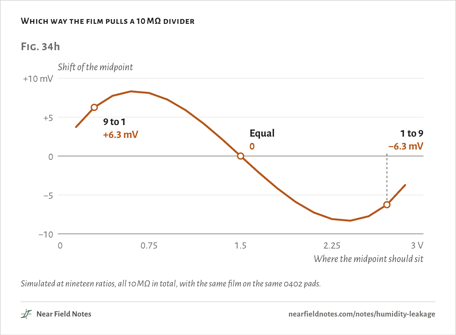
A film that leaks the same across both resistors leaves an equal divider where it is. An unequal one is pulled toward half the supply.

These numbers are the mild end. Real residue collects at the joints, where it does the most harm.

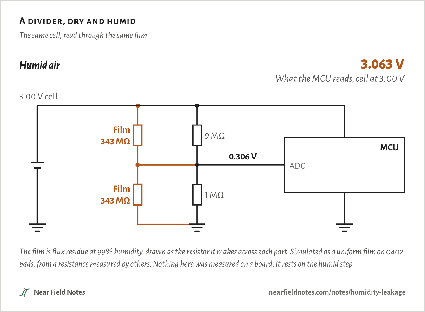
A divider, dry and humid

The same cell, read through the same film

Dry board3.000 V9 MΩ1 MΩ0.300 VHumid air3.063 V9 MΩ1 MΩ0.306 VFilm343 MΩFilm343 MΩHumid, a 1 MΩ divider3.006 V900 kΩ100 kΩ0.301 VFilm343 MΩFilm343 MΩWhat the MCU reads, cell at 3.00 VMCUADC3.00 V cellDry board3.000 V9 MΩ1 MΩ0.300 VHumid air3.063 V9 MΩ1 MΩ0.306 VFilm343 MΩFilm343 MΩHumid, a 1 MΩ divider3.006 V900 kΩ100 kΩ0.301 VFilm343 MΩFilm343 MΩWhat the MCU reads, cell at 3.00 VMCUADC3.00 V cellDry board3.000 V9 MΩ1 MΩ0.300 VHumid air3.063 V9 MΩ1 MΩ0.306 VFilm343 MΩFilm343 MΩHumid, a 1 MΩ divider3.006 V900 kΩ100 kΩ0.301 VFilm343 MΩFilm343 MΩWhat the MCU reads, cell at 3.00 VMCUADC3.00 V cell
The film is flux residue at 99% humidity, drawn as the resistor it makes across each part. Simulated as a uniform film on 0402 pads, from a resistance measured by others. Nothing here was measured on a board. It rests on the humid step.

A coin cell board that reads its own battery

44 × 24 mm, 3.00 V

Take a Bluetooth sensor board that runs for years on a CR2032 coin cell. To know when the cell is dying, its microcontroller measures the cell’s voltage.

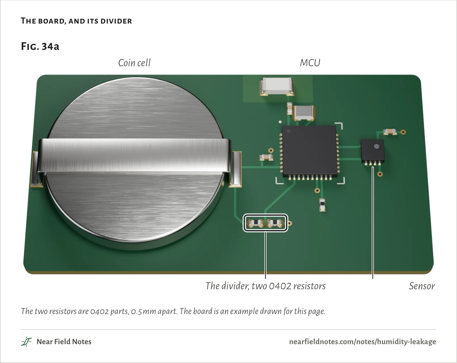
Two resistors do the scaling. They sit end to end between the cell and ground, and one ADC pin reads the point between them.

The board, and its divider
Fig. 34aCoin cellMCUThe divider, two 0402 resistorsSensorFig. 34aCoin cellMCUThe divider, two 0402 resistorsSensorFig. 34aCoin cellMCUThe divider, two 0402 resistorsSensor
The two resistors are 0402 parts, 0.5 mm apart. The board is an example drawn for this page.
The numbers
PartWhat it is
Coin cellA CR2032 under a retainer strap, 3.00 V, 225 mAh assumed
MCUA Bluetooth microcontroller with its crystal and chip antenna. One ADC pin reads the divider
Divider9 MΩ from the cell to the midpoint, 1 MΩ from the midpoint to ground, both 0402, 0.5 mm apart
SensorA temperature and humidity sensor on the microcontroller’s bus

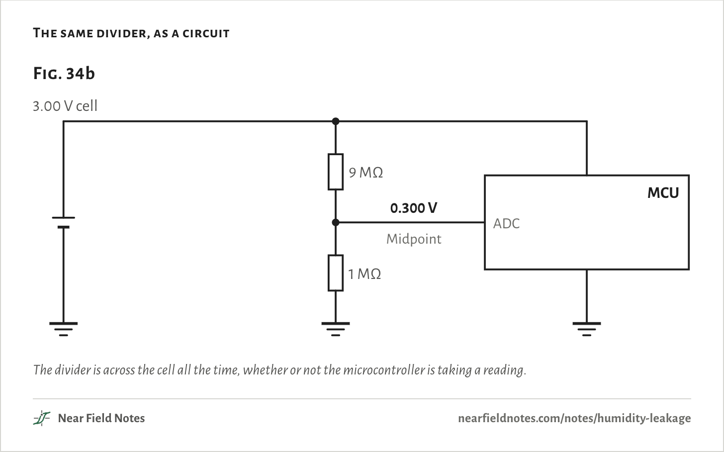
As a circuit: 9 MΩ from the cell to the midpoint, and 1 MΩ from the midpoint to ground. The midpoint sits at a tenth of the cell, 0.300 V, and the firmware multiplies by ten.

Nothing else is on the midpoint but the ADC pin. Every path from it to another net is supposed to be one of the two resistors.

The same divider, as a circuit
Fig. 34b9 MΩ1 MΩ0.300 VMCUADC3.00 V cellMidpointFig. 34b9 MΩ1 MΩ0.300 VMCUADC3.00 V cellMidpointFig. 34b9 MΩ1 MΩ0.300 VMCUADC3.00 V cellMidpoint
The divider is across the cell all the time, whether or not the microcontroller is taking a reading.

Why the resistors get so large

0.3 µA at 10 MΩ

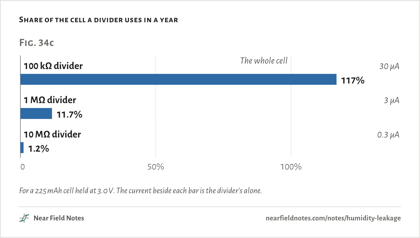
The divider draws current every hour of the year. At 100 kΩ in all that is 30 µA, which empties a 225 mAh cell in about 10 months by itself.

At 1 MΩ it takes 11.7% of the cell each year. At 10 MΩ it takes 1.2%. So on a board meant to last years, the divider grows until its current stops mattering.

What grows with it is how little it takes to move the midpoint. Any stray path of a few hundred megohms now counts.

Share of the cell a divider uses in a year
Fig. 34c050%100%100 kΩ divider117%30 µA1 MΩ divider11.7%3 µA10 MΩ divider1.2%0.3 µAWhole cellFig. 34c050%100%100 kΩ divider117%30 µA1 MΩ divider11.7%3 µA10 MΩ divider1.2%0.3 µAThe whole cellFig. 34c050%100%100 kΩ divider117%30 µA1 MΩ divider11.7%3 µA10 MΩ divider1.2%0.3 µAThe whole cell
For a 225 mAh cell held at 3.0 V. The current beside each bar is the divider’s alone.
The numbers

The cell held at 3.0 V all year, 225 mAh assumed. Arithmetic, not a simulation.

DividerCurrentCharge in a yearShare of the cell
100 kΩ30 µA262.8 mAh116.8%
1 MΩ3 µA26.3 mAh11.7%
10 MΩ0.3 µA2.6 mAh1.2%

The board isn’t the leak

Clean FR-4, over 100 GΩ

The first suspect is the board itself, taking up water. Jack Ganssle measured that. Across a 1 cm gap of clean, bare FR-4 at 80% humidity he found 20 pA, which is about 165 GΩ.

Put that across the 9 MΩ resistor and the reading moves by 0.005%. With solder mask over the copper he measured under 10 fA, even with the board wet.

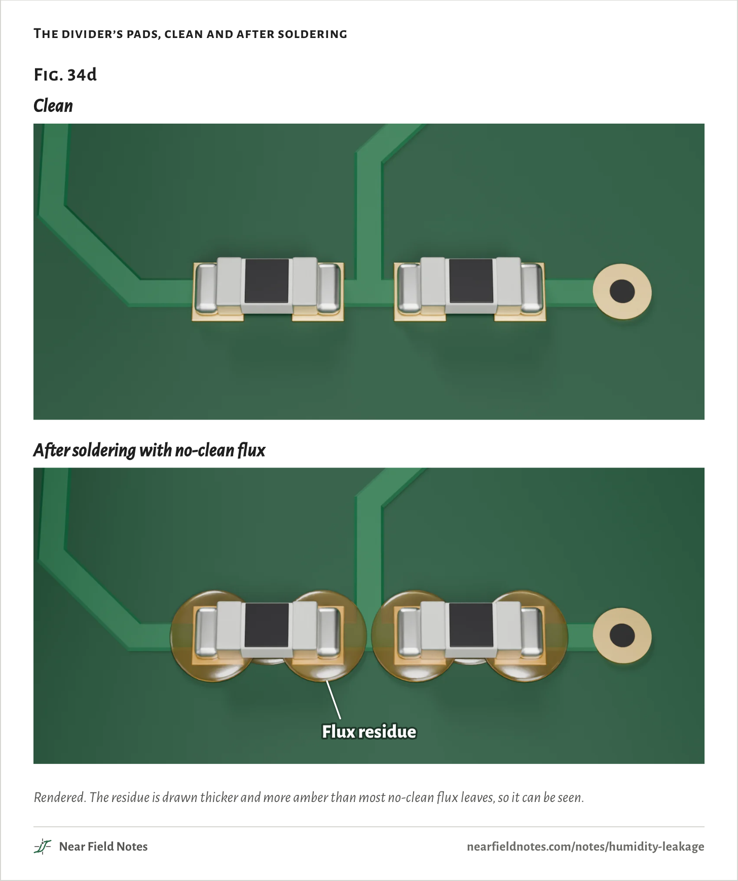
The leak is what soldering leaves behind. No-clean flux leaves a ring of weak organic acids around every joint. Dry, they insulate.

The divider’s pads, clean and after soldering
Fig. 34dCleanAfter soldering with no-clean fluxFlux residueFig. 34dCleanAfter soldering with no-clean fluxFlux residueFig. 34dCleanAfter soldering with no-clean fluxFlux residue
Rendered. The residue is drawn thicker and more amber than most no-clean flux leaves, so it can be seen.
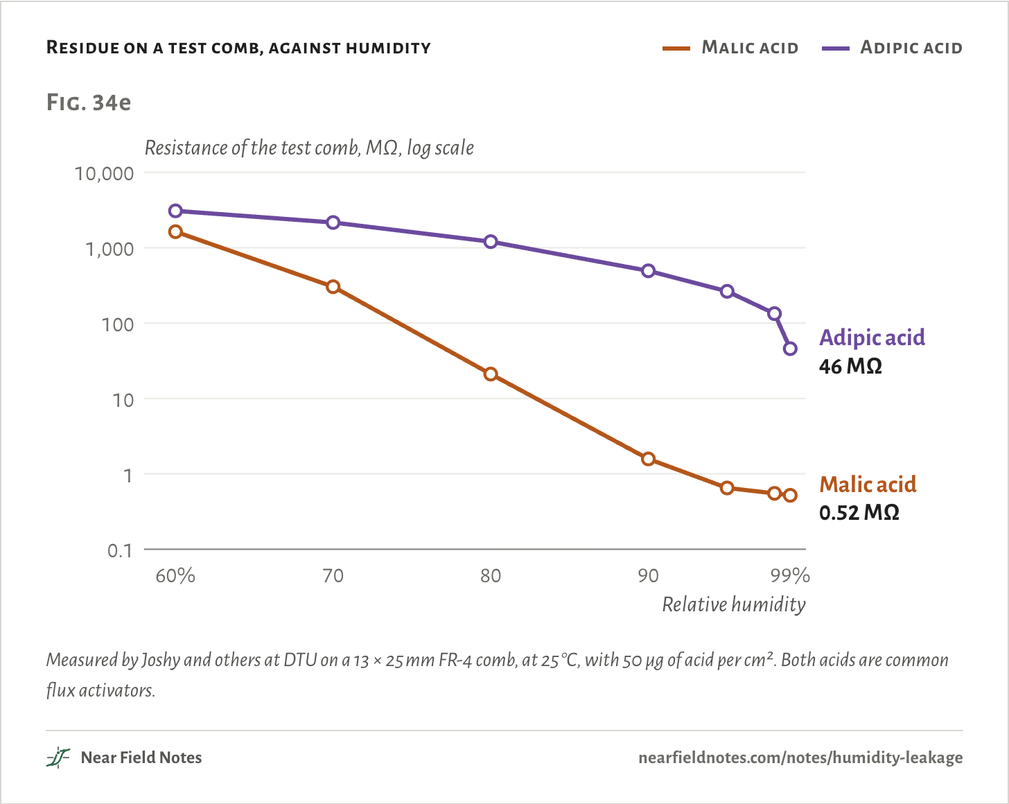
Residue on a test comb, against humidity
  • Malic acid
  • Adipic acid
Fig. 34eResistance of the test comb, MΩ, log scale0.11101001,00010,000Adipic acid46 MΩMalic acid0.52 MΩ60%70809099%Relative humidityFig. 34eResistance of the test comb, MΩ, log scale0.11101001,00010,000Adipic acid46 MΩMalic acid0.52 MΩ60%70809099%Relative humidityFig. 34eResistance of the test comb, MΩ, log scale0.11101001,00010,000Adipic acid46 MΩMalic acid0.52 MΩ60%70809099%Relative humidity
Measured by Joshy and others at DTU on a 13 × 25 mm FR-4 comb, at 25 °C, with 50 µg of acid per cm². Both acids are common flux activators.
The numbers

Megohms across the comb at 25, 50 and 75 µg of acid per cm², 25 °C. From Joshy et al. 2019, Tables 1 and 2. The figure draws the 50 µg/cm² columns.

HumidityAdipic, 25Adipic, 50Adipic, 75Malic, 25Malic, 50Malic, 75
60%5,2093,0902,7892,9021,635602.4
70%4,9452,1581,6652,587303.739.93
80%2,8661,205922.52,07121.123.18
90%504.2494.6449.6781.91.580.42
95%209.7263.5293.21510.650.32
98%157.3133.7194.930.830.550.32
99%102.845.7323.796.620.520.28
602

The film is a resistor across each part

343 MΩ each

To put a number on one divider, spread that wet residue as an even film over the pads and solve for the current in it. At 99% humidity DTU’s comb works out to 939 MΩ for each square of film. A square of film has the same resistance from edge to edge at any size, so a film is counted in squares.

Between the two pads of one 0402 part, the film is worth 2.74 such squares side by side. That makes it a 343 MΩ resistor across the part.

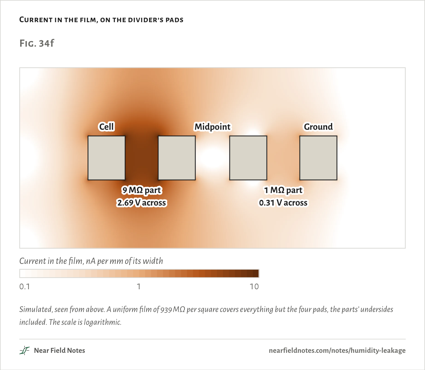
The film is the same across both parts. The voltage is not: 2.69 V sits across the 9 MΩ part and 0.31 V across the 1 MΩ part, so about nine times the current runs in the film under the first.

Current in the film, on the divider’s pads
Fig. 34fCellMidpointGround9 MΩ part2.69 V across1 MΩ part0.31 V acrossCurrent in the film, nA per mm of its width0.1110Fig. 34fCellMidpointGround9 MΩ part2.69 V across1 MΩ part0.31 V acrossCurrent in the film, nA per mm of its width0.1110Fig. 34fCellMidpointGround9 MΩ part2.69 V across1 MΩ part0.31 V acrossCurrent in the film, nA per mm of its width0.1110
Simulated, seen from above. A uniform film of 939 MΩ per square covers everything but the four pads, the parts’ undersides included. The scale is logarithmic.

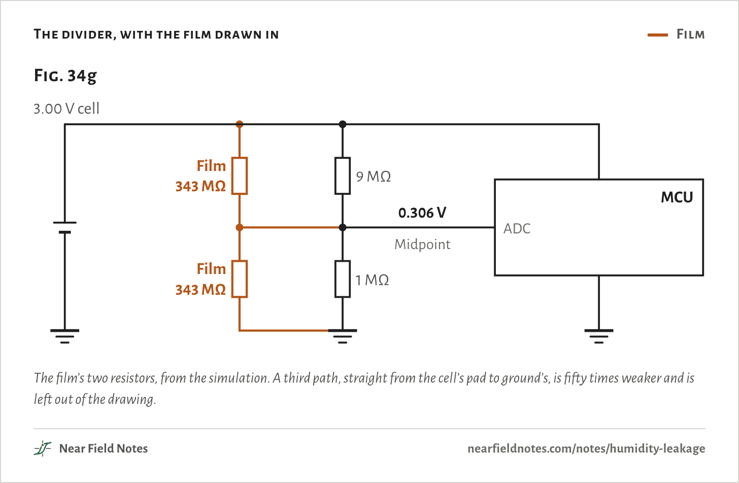
So the circuit gains two resistors. Each real resistor now has 343 MΩ in parallel with it.

Vmid=VRb ∥ RfRt ∥ Rf + Rb ∥ Rf

343 MΩ hardly changes 1 MΩ. It takes 2.6% off 9 MΩ. The top of the divider gets smaller, the midpoint rises by 6.3 mV to 0.306 V, and a 3.00 V cell reads 3.063 V.

The extra current is nothing: 7 nA more from the cell. What the film costs is accuracy.

The divider, with the film drawn in
  • Film
Fig. 34g9 MΩ1 MΩ0.306 VFilm343 MΩFilm343 MΩMCUADC3.00 V cellMidpointFig. 34g9 MΩ1 MΩ0.306 VFilm343 MΩFilm343 MΩMCUADC3.00 V cellMidpointFig. 34g9 MΩ1 MΩ0.306 VFilm343 MΩFilm343 MΩMCUADC3.00 V cellMidpoint
The film’s two resistors, from the simulation. A third path, straight from the cell’s pad to ground’s, is fifty times weaker and is left out of the drawing.
Which way the film pulls a 10 MΩ divider
Fig. 34hShift of the midpoint−10−50+5+10 mV9 to 1+6.3 mVEqual01 to 9−6.3 mV00.751.52.253 VWhere the midpoint should sitFig. 34hShift of the midpoint−10−50+5+10 mV9 to 1+6.3 mVEqual01 to 9−6.3 mV00.751.52.253 VWhere the midpoint should sitFig. 34hShift of the midpoint−10−50+5+10 mV9 to 1+6.3 mVEqual01 to 9−6.3 mV00.751.52.253 VWhere the midpoint should sit
Simulated at nineteen ratios, all 10 MΩ in total, with the same film on the same 0402 pads.
The numbers

10 MΩ in all, 0402 parts, film of 939 MΩ per square, 3.00 V cell.

Midpoint should beDividerIt moves byError in the reading
0.15 V9.5 MΩ over 500 kΩ+3.73 mV+2.48%
0.30 V9 MΩ over 1 MΩ+6.26 mV+2.09%
0.75 V7.5 MΩ over 2.5 MΩ+8.11 mV+1.08%
1.50 V5 MΩ over 5 MΩ00
2.25 V2.5 MΩ over 7.5 MΩ−8.11 mV−0.36%
2.70 V1e+03 kΩ over 9 MΩ−6.26 mV−0.23%
2.85 V500 kΩ over 9.5 MΩ−3.73 mV−0.13%
604

A bigger part doesn’t fix it

3.1% to 1.3%

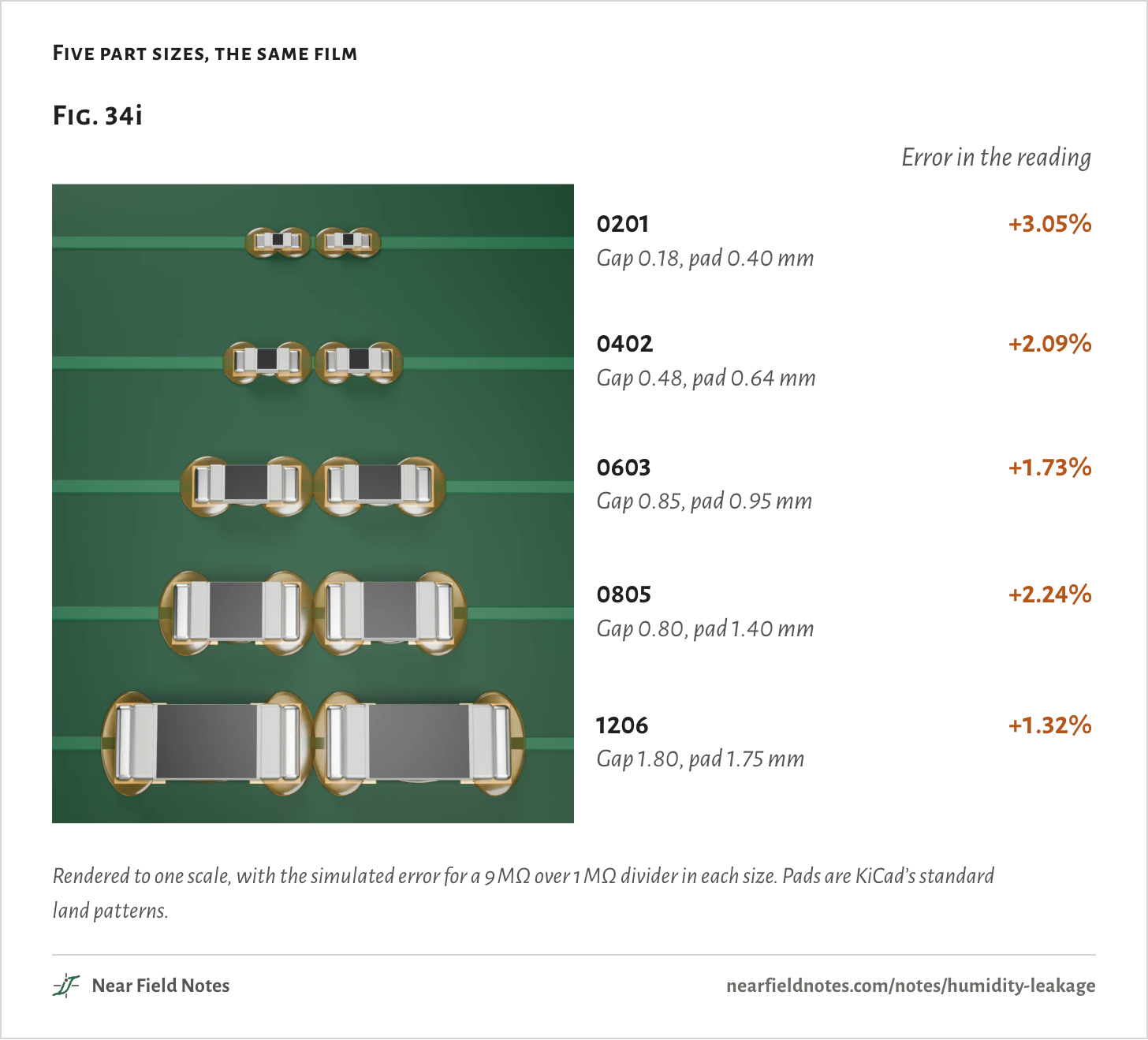
The usual advice for leakage is distance: use a longer part and the path gets longer. A 1206 has a gap of 1.80 mm between its pads, against 0.48 mm for an 0402.

Its pads are also wider, 1.75 mm against 0.64 mm. The film between them is a longer path and a wider one, and the two nearly cancel.

Five part sizes, the same film
Fig. 34i0201+3.05%0402+2.09%0603+1.73%0805+2.24%1206+1.32%Fig. 34iError in the reading0201+3.05%Gap 0.18, pad 0.40 mm0402+2.09%Gap 0.48, pad 0.64 mm0603+1.73%Gap 0.85, pad 0.95 mm0805+2.24%Gap 0.80, pad 1.40 mm1206+1.32%Gap 1.80, pad 1.75 mmFig. 34iError in the reading0201+3.05%Gap 0.18, pad 0.40 mm0402+2.09%Gap 0.48, pad 0.64 mm0603+1.73%Gap 0.85, pad 0.95 mm0805+2.24%Gap 0.80, pad 1.40 mm1206+1.32%Gap 1.80, pad 1.75 mm
Rendered to one scale, with the simulated error for a 9 MΩ over 1 MΩ divider in each size. Pads are KiCad’s standard land patterns.
The numbers

9 MΩ over 1 MΩ, film of 939 MΩ per square, 3.00 V cell. Pads are KiCad’s. Squares are for one footprint alone. The film across each part is in the divider’s layout.

SizeGapPad widthSquares, one partFilm across each partErrorReads
02010.18 mm0.40 mm4.16234 MΩ+3.05%3.092 V
04020.48 mm0.64 mm2.92343 MΩ+2.09%3.063 V
06030.85 mm0.95 mm2.48415 MΩ+1.73%3.052 V
08050.80 mm1.40 mm3.16320 MΩ+2.24%3.067 V
12061.80 mm1.75 mm1.94542 MΩ+1.32%3.040 V
606

What layout can do

A slot, and what sits nearby

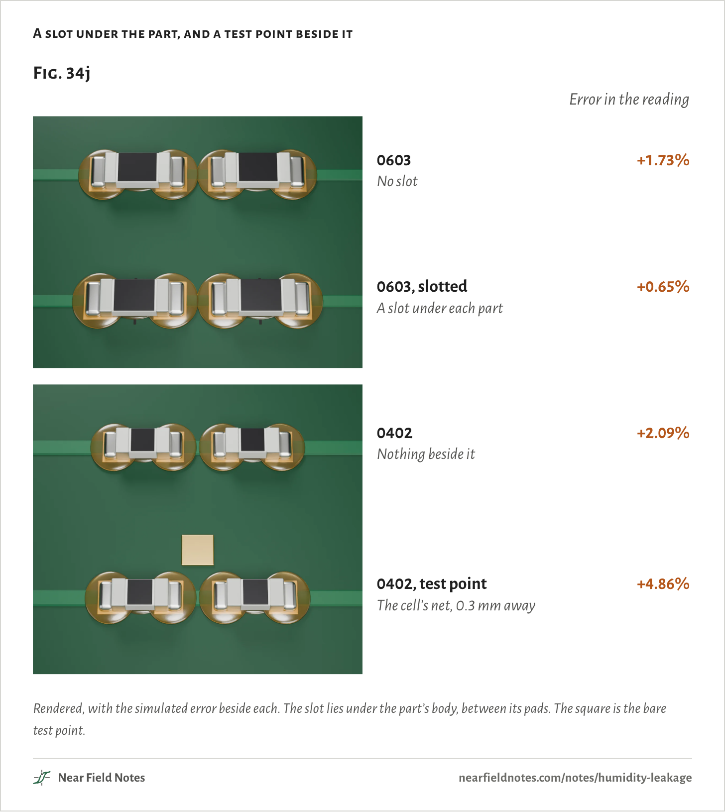
A slot milled through the board under each part takes away the surface the film would lie on. Under 0603 parts it cuts the error from 1.73% to 0.65%. The film still reaches around the slot’s ends.

What sits beside the midpoint matters more than the parts. A bare test point on the cell’s net, 0.3 mm from the midpoint’s pads, is one more path down from the cell. The error goes from 2.09% to 4.86%.

The same test point on ground pulls the other way, and the error falls to 1.50%. Either one breaks the balance, so an equal divider beside it now moves by 0.9%.

Copper under solder mask doesn’t touch the film. Keep the midpoint short, cover what can be covered, and leave no bare copper of another net next to it.

A slot under the part, and a test point beside it
Fig. 34j0603+1.73%0603, slotted+0.65%0402+2.09%0402, test point+4.86%Fig. 34jError in the reading0603+1.73%No slot0603, slotted+0.65%A slot under each part0402+2.09%Nothing beside it0402, test point+4.86%The cell’s net, 0.3 mm awayFig. 34jError in the reading0603+1.73%No slot0603, slotted+0.65%A slot under each part0402+2.09%Nothing beside it0402, test point+4.86%The cell’s net, 0.3 mm away
Rendered, with the simulated error beside each. The slot lies under the part’s body, between its pads. The square is the bare test point.
The numbers

10 MΩ in all, film of 939 MΩ per square, 3.00 V cell. A slot is the pads’ width plus 0.6 mm, 0.2 mm clear of the copper. A test point is a 0.6 mm bare square.

LayoutFilm, cell to midpointError, 9 to 1ReadsError, equal legsExtra from the cell
0603415 MΩ+1.73%3.052 V06.0 nA
0603, slot under each part1.1 GΩ+0.65%3.020 V02.3 nA
1206542 MΩ+1.32%3.040 V04.5 nA
1206, slot under each part1.73 GΩ+0.42%3.012 V01.4 nA
0402343 MΩ+2.09%3.063 V07.3 nA
0402, test point of the cell’s net158 MΩ+4.86%3.146 V+0.92%17.5 nA
0402, test point of ground389 MΩ+1.50%3.045 V−0.92%8.5 nA

A smaller divider, switched

0.21% at 1 MΩ, 0.02% at 100 kΩ

The film is a fixed few hundred megohms. Make the divider ten times smaller and the film moves it ten times less: 0.21% at 1 MΩ, where a 3.00 V cell reads 3.006 V, and 0.021% at 100 kΩ.

Humidity does the rest. Below 70% this residue moves even the 10 MΩ divider by less than 0.01%. Between 70 and 90% the error grows more than a hundredfold.

That is the answer to how big. At 1 MΩ the worst of it is 6 mV on the reading. At 10 MΩ it is 63 mV.

Error in the reading, against humidity
Fig. 34kError in the reading, log scale0.0001%0.01%1%10 MΩ+2.09%1 MΩ+0.21%100 kΩ+0.021%60%70809099%Relative humidityFig. 34kError in the reading, log scale0.0001%0.01%1%10 MΩ+2.09%1 MΩ+0.21%100 kΩ+0.021%60%70809099%Relative humidityFig. 34kError in the reading, log scale0.0001%0.01%1%10 MΩ+2.09%1 MΩ+0.21%100 kΩ+0.021%60%70809099%Relative humidity
Simulated for 9 to 1 dividers on 0402 parts, with a film set by DTU’s malic-acid comb at each humidity.
The numbers

Malic acid, 50 µg/cm², 9 to 1 dividers on 0402 parts. The last column takes the comb’s 0.3 mm pitch as line plus gap, which makes the film four times as resistive.

HumidityDTU’s combFilm, per square10 MΩ1 MΩ100 kΩ10 MΩ, other reading
60%1,635 MΩ2,950 GΩ+0.00067%+0.000067%+0.0000067%+0.00017%
70%303.7 MΩ548 GΩ+0.0036%+0.00036%+0.000036%+0.00090%
80%21.12 MΩ38.1 GΩ+0.052%+0.0052%+0.00052%+0.013%
90%1.58 MΩ2.85 GΩ+0.69%+0.069%+0.0069%+0.17%
95%0.65 MΩ1.17 GΩ+1.67%+0.17%+0.017%+0.42%
98%0.55 MΩ993 MΩ+1.97%+0.20%+0.020%+0.50%
99%0.52 MΩ939 MΩ+2.09%+0.21%+0.021%+0.52%

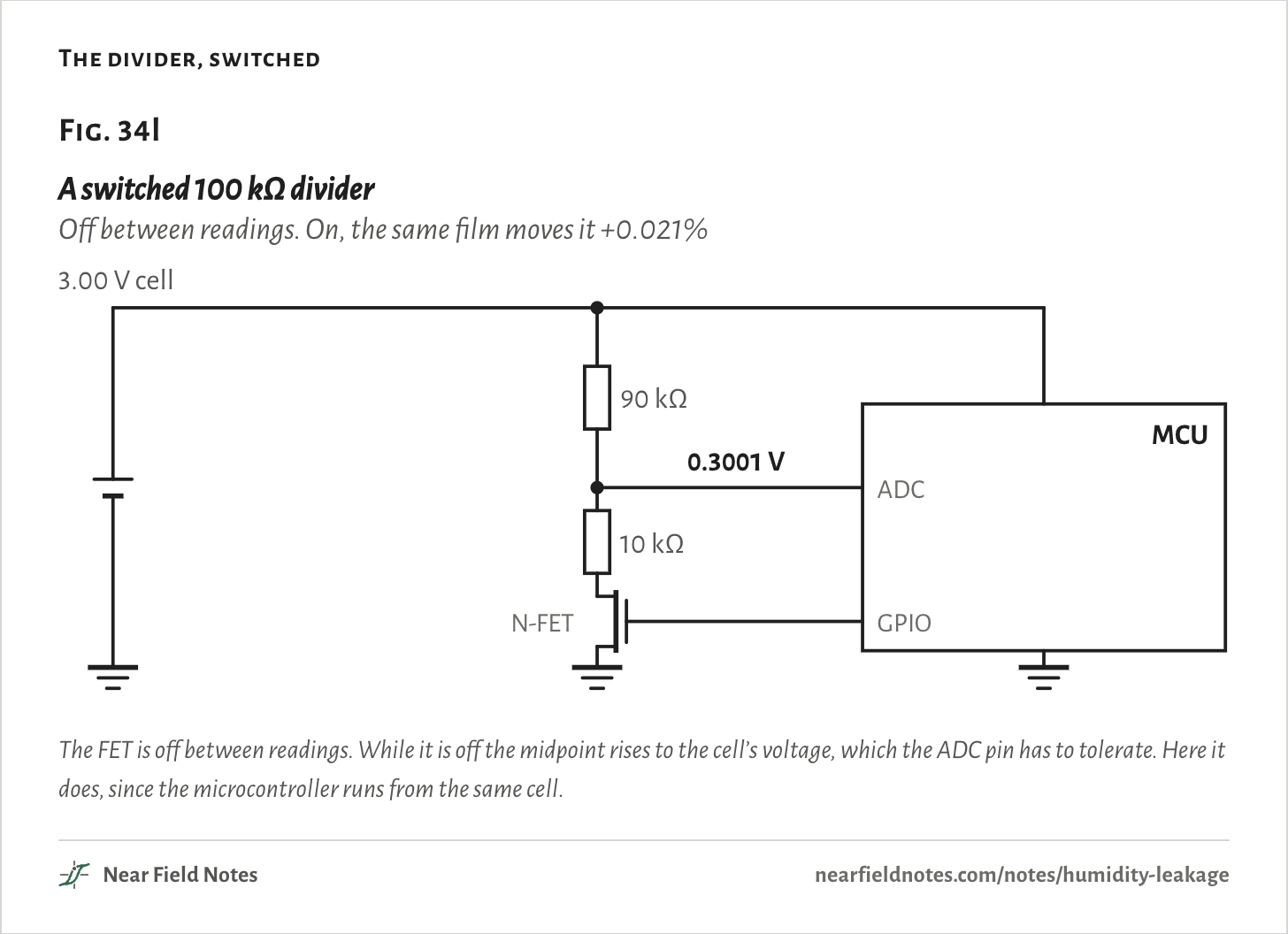
A 100 kΩ divider left on empties the cell in 10 months. So switch it. A small FET under the bottom resistor connects the divider only while the microcontroller takes a reading, and the rest of the time it draws nothing.

Or leave the divider out. Many microcontrollers can measure their own supply against a reference inside the chip. On Nordic’s nRF52832 the ADC takes the supply pin as an input, with no parts on the board for a film to bridge.

Some regulators avoid the problem the same way. TI’s TPS62840 and Analog Devices’ MAX17222 each set their output from one resistor that they read once at start-up, and then ignore.

The divider, switched
Fig. 34lA switched 100 kΩ dividerOff between readings. Film: +0.021%90 kΩ10 kΩ0.3001 VGPION-FETMCUADC3.00 V cellFig. 34lA switched 100 kΩ dividerOff between readings. On, the same film moves it +0.021%90 kΩ10 kΩ0.3001 VGPION-FETMCUADC3.00 V cellFig. 34lA switched 100 kΩ dividerOff between readings. On, the same film moves it +0.021%90 kΩ10 kΩ0.3001 VGPION-FETMCUADC3.00 V cell
The FET is off between readings. While it is off the midpoint rises to the cell’s voltage, which the ADC pin has to tolerate. Here it does, since the microcontroller runs from the same cell.

Clean the board properly, or coat it

A wipe can make it worse

No residue, no film. A board that is washed well after soldering goes back to the clean laminate’s hundreds of gigohms.

A quick wipe is not a wash. It dissolves the residue and spreads it thin across the gaps it used to sit beside. Ganssle wiped a rosin-flux board with isopropyl alcohol and its leakage went from 2 pA to 32 pA, until a second, more careful cleaning.

A conformal coating keeps liquid water off the copper. It also seals in whatever is under it, so it goes on a clean board.

The same film is behind another fault. A 32 kHz watch crystal’s oscillator runs on so little current that a leak across its pins can slow its start or stop it. TI’s guide to those oscillators names moisture drawn to flux residue as a cause.

Note 33 follows a different leak on a board like this one, through the bus pins of a sensor that is switched off.

Which divider?

Three questions

The choice comes down to what the microcontroller can do by itself, whether it has a pin to spare, and how much error the reading can take.

Key to a battery reading on a coin cell

Is a divider needed, and how large can it be?

  1. 1aThe microcontroller can measure its own supplyNo divider
  2. 1bIt can’t, or the voltage is above its supplyGo to 2
  3. 2aA pin is free to switch the divider100 kΩ, switched
  4. 2bNo pin is freeGo to 3
  5. 3a0.21% in damp air and 11.7% of the cell a year are acceptable1 MΩ, left on
  6. 3bThey aren’t10 MΩ, on a washed or coated board

The board in Fig. 34a ends at 1a. Its microcontroller runs straight from the cell and can measure its own supply.

Conditions

Simulated
Every error and reading on this page comes from a simulation of a film on the board’s surface. None was measured on a board.
Film
A uniform sheet of 939 MΩ per square over the whole patch of board, under the parts included. Bare pads are perfect conductors. Copper under solder mask doesn’t touch the film.
Where 939 MΩ comes from
DTU’s measured comb with malic acid, 50 µg/cm², at 99% humidity and 25 °C: 0.52 MΩ. The comb is 13 × 25 mm with a 0.3 mm pitch. Read as 0.3 mm lines and 0.3 mm gaps, it is 1,806 squares of film side by side.
Divider
9 MΩ over 1 MΩ on a 3.00 V source, unless a figure says otherwise. The ADC pin draws nothing.
Pads
KiCad’s standard land patterns for 0201 to 1206 chip resistors. The two parts sit end to end with 0.5 mm between the midpoint’s two pads, which a trace under solder mask joins.
Slot
Under each part, between its pads, 0.2 mm clear of the copper and 0.6 mm longer than the pads are wide. No film in it.
Test point
A bare 0.6 mm square, 0.3 mm from the midpoint’s pads.
Solver
A finite-difference solve of the film’s potential on a 10 µm grid, which gives the conductance between each pair of nets. Going from a 20 µm grid to a 5 µm one moves one 0402 footprint’s figure from 2.86 to 2.94 squares.
Battery use
Arithmetic: 3.0 V across the divider all year, and a 225 mAh cell.
Clean board
Ganssle’s 20 pA is converted to 165 GΩ at the 3.3 V his text implies.
Render
Blender. The board is an example drawn for this page, with generic parts.

Simulated from others’ measurements. Nothing on this page has been measured on a board.

Limits

  • A uniform film is the mild end. DTU measured real 0402, 0603 and 0805 land patterns within ten times its comb’s resistance for one acid. With ten times the comb across each part, this divider is off by 3.4% at 80% humidity and 41% at 90%.
  • The paper doesn’t say whether the comb’s 0.3 mm pitch is the gap or the line plus the gap. Read the second way, the film is four times as resistive and the 10 MΩ error at 99% is 0.52%.
  • One residue stands for all. Malic acid starts to dissolve near 80% humidity. An adipic-acid flux stays dry to about 98%, and commercial blends differ.
  • Breath is not simulated. Condensed water is wetter than 99% humidity, and how much residue it dissolves was not modeled.
  • The film has no time in it. A real one takes minutes to form and dries out at a lower humidity than it formed at.
  • Leakage through the laminate and inside the parts is left out, and so is the ADC pin’s own leakage.

Files

  • sim/film.pyThe film solver, the land patterns, DTU’s table and every layout
  • sim/site.pyThe same solver’s runs for this page: by humidity, by ratio, and the current map
  • render/scene.pyThe board and the test coupons in Blender

Sources

Like this note?

Rev 1 ·
  1. Rev 1First published

Each fix gets a line here, with the reader's name if they want credit.

Did it answer your question?

Want more on this?

Report a problem

What should the next note be? Ask for one