Near Field Notes

Note 16Signal integrityRev 1Watch the video · 0:14

TDR

How do you read a TDR trace?

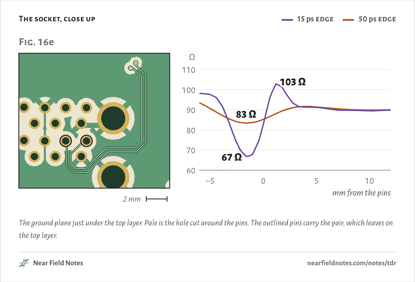
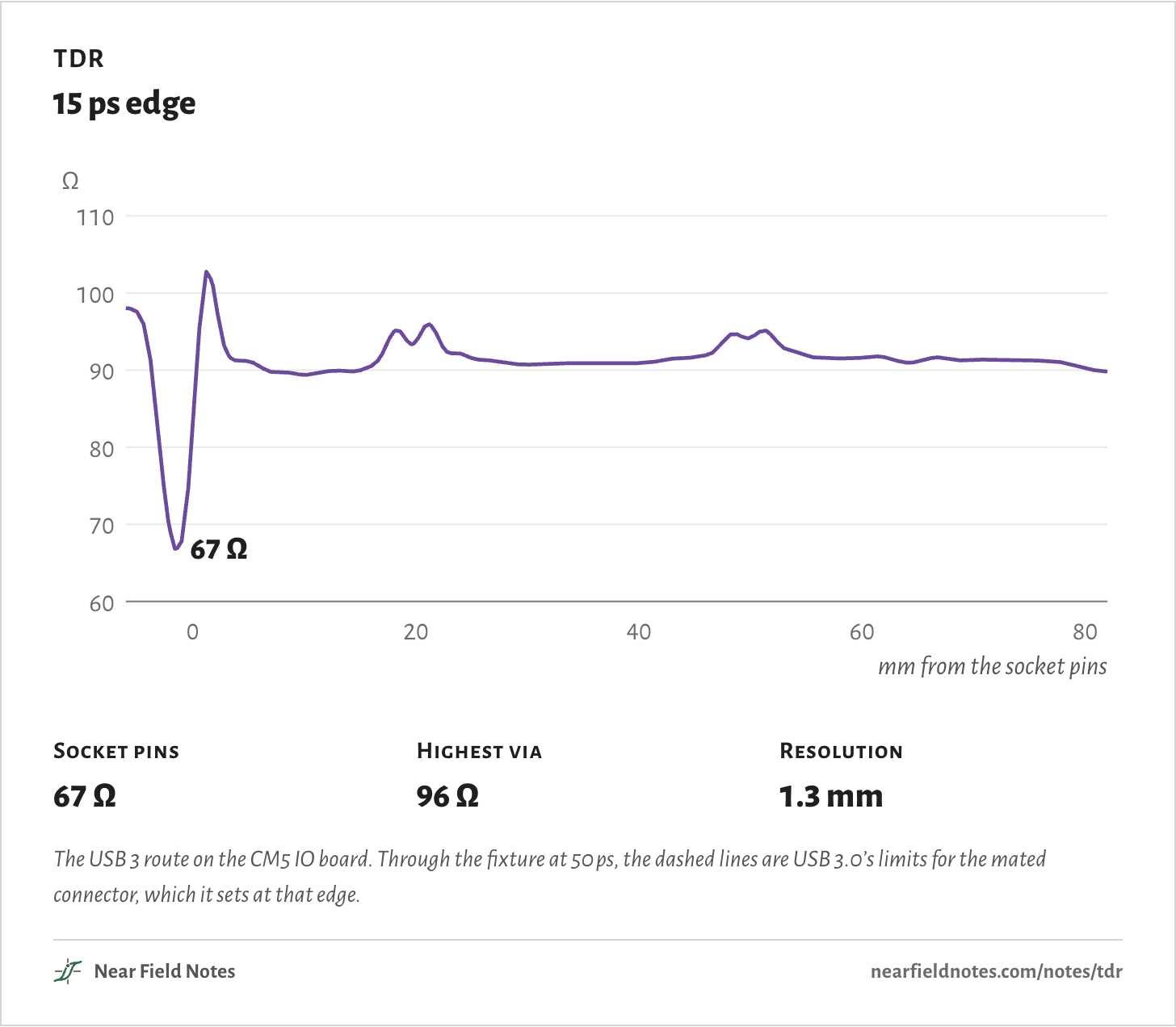
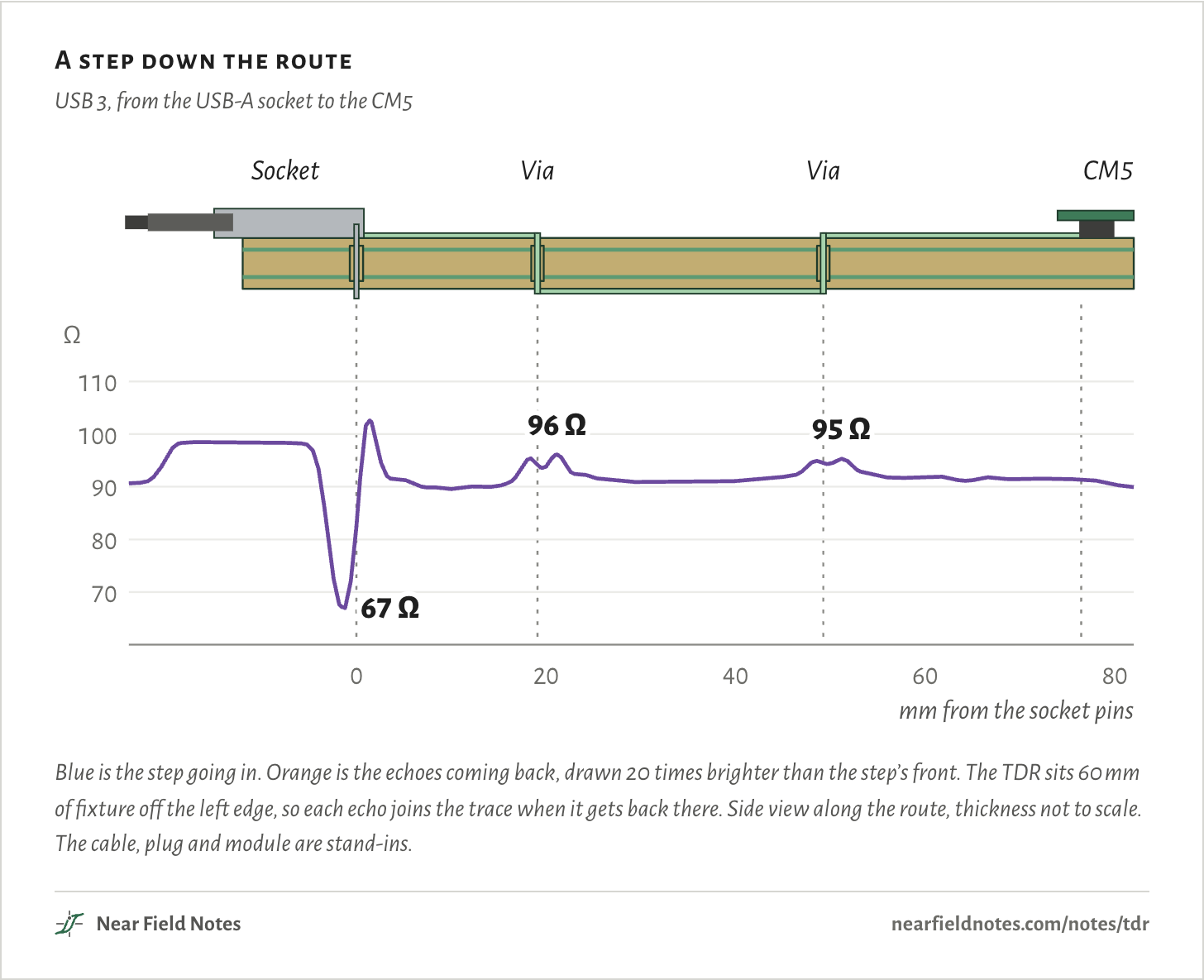
As a map of the route. Across is distance: on this board, every 11.8 ps of echo time is 1 mm of trace. Up is impedance: a dip is extra capacitance, and a bump is extra inductance or a broken return path. Read it with the edge your spec names. The CM5 IO board’s USB-A socket pins read 67 Ω with a 15 ps edge and 83 Ω with USB 3.0’s 50 ps, inside its 90 ± 15 Ω.

A TDR sends a fast step down a line and records what comes back. Every change in the line sends part of the step back, and the time it takes says where.

The figure follows a 15 ps step down the USB 3 receive pair of Raspberry Pi’s CM5 IO board.

A step down the route

USB 3, from the USB-A socket to the CM5

SocketViaViaCM5708090100110020406080mm from the socket pinsΩ67 Ω96 Ω95 ΩSocketViaViaCM5708090100110020406080mm from the socket pinsΩ67 Ω96 Ω95 ΩSocketViaViaCM5708090100110020406080mm from the socket pinsΩ67 Ω96 Ω95 Ω
Blue is the step going in. Orange is the echoes coming back, drawn 20 times brighter than the step’s front. The TDR sits 60 mm of fixture off the left edge, so each echo joins the trace when it gets back there. Side view along the route, thickness not to scale. The cable, plug and module are stand-ins.
The numbers
What a 15 ps edge reads along the route, through 60 mm of fixture. A peak or dip can sit about 2 mm from the copper that causes it.
PlaceRead at, mm from the pinsTDR reads
Socket pins−1.267 Ω
Hole in the plane past the pins1.4103 Ω
First via pair21.296 Ω
Plain line, bottom layer2891 Ω
Second via pair51.295 Ω

What a TDR is

A step, a scope and a line

A TDR is a step source and a fast scope on the same wire. The step rises in a few tens of picoseconds and runs down the line. Wherever the line’s impedance changes, part of it reflects.

The scope adds each echo to the step it sent. Its trace rises where the line’s impedance goes up and falls where it goes down. A fast trace is built to hold one impedance all the way: 90 Ω for USB 3, 100 Ω for HDMI and DisplayPort. A flat trace means a clean route.

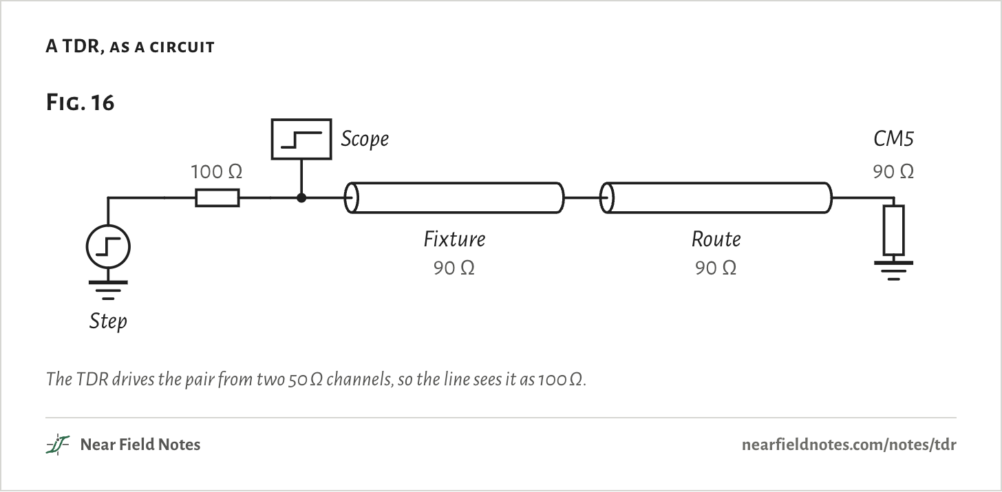
A TDR, as a circuit
Fig. 16100 ΩScopeStepFixture90 ΩRoute90 Ω90 ΩCM5Fig. 16100 ΩScopeStepFixture90 ΩRoute90 Ω90 ΩCM5Fig. 16100 ΩScopeStepFixture90 ΩRoute90 Ω90 ΩCM5
The TDR drives the pair from two 50 Ω channels, so the line sees it as 100 Ω.
The parts
Each part of the circuit, left to right.
PartValue
Step source and its resistance100 Ω
Fixture90 Ω, 60 mm
Route on the board90 Ω, 76 mm
CM5 receiver90 Ω

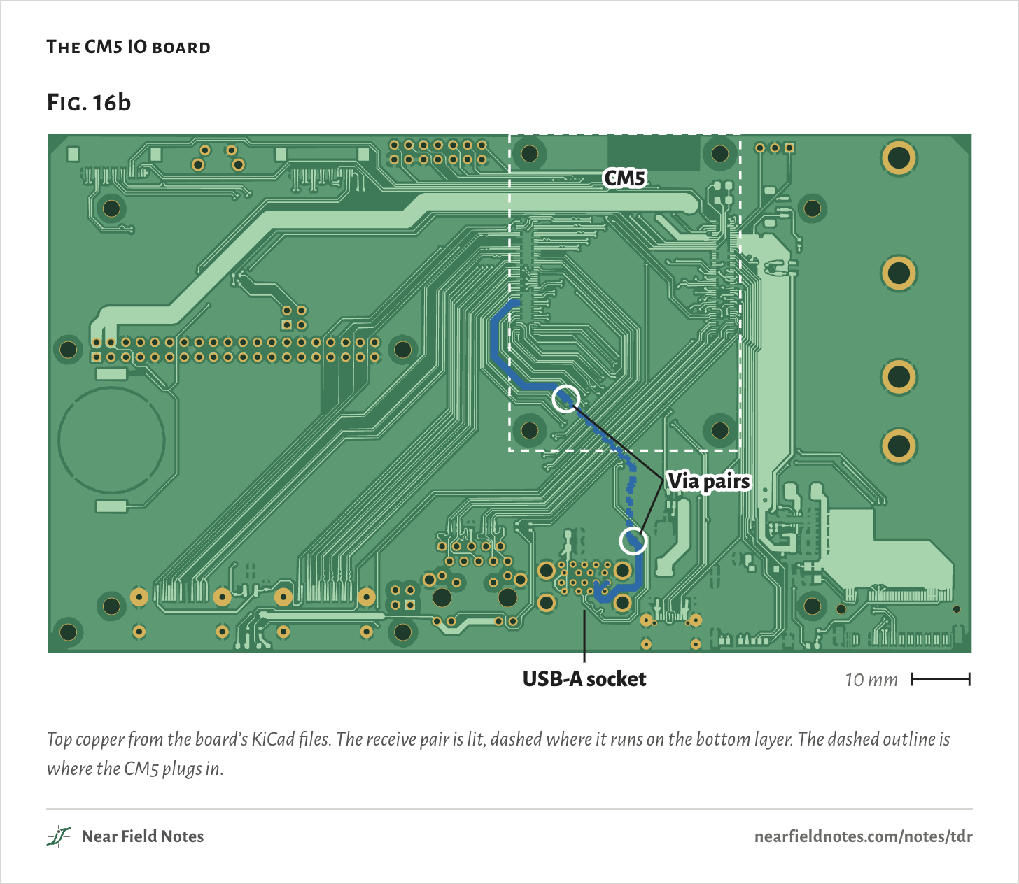
The route here is real. Raspberry Pi publishes the KiCad files of its CM5 IO board, a 4-layer, 1.6 mm board. Its USB 3 receive pair runs 76 mm from the USB-A socket to the CM5 module.

On the way it drops to the bottom layer through one via pair and comes back up through another. Every trace of the USB 3 route comes from that copper. The cable, the plug and the module have no design files here, so they’re stand-ins.

The CM5 IO board
Fig. 16bCM5USB-A socketVia pairs10 mmFig. 16bCM5USB-A socketVia pairs10 mmFig. 16bCM5USB-A socketVia pairs10 mm
Top copper from the board’s KiCad files. The receive pair is lit, dashed where it runs on the bottom layer. The dashed outline is where the CM5 plugs in.
The route
The USB 3 receive pair, from the socket pins.
StretchLayerLength
Socket pins to the first via pairTop19.1 mm
Between the via pairsBottom30.15 mm
Second via pair to the moduleTop27.2 mm

Reading the trace

Up is impedance

The scope measures how much of the step comes back. That share is the reflection coefficient. Against the TDR’s own 100 Ω, it turns into impedance:

Z=ZTDR1 + ρ1 − ρ

=100 Ω × 0.802 / 1.198=67 Ωat the socket pins

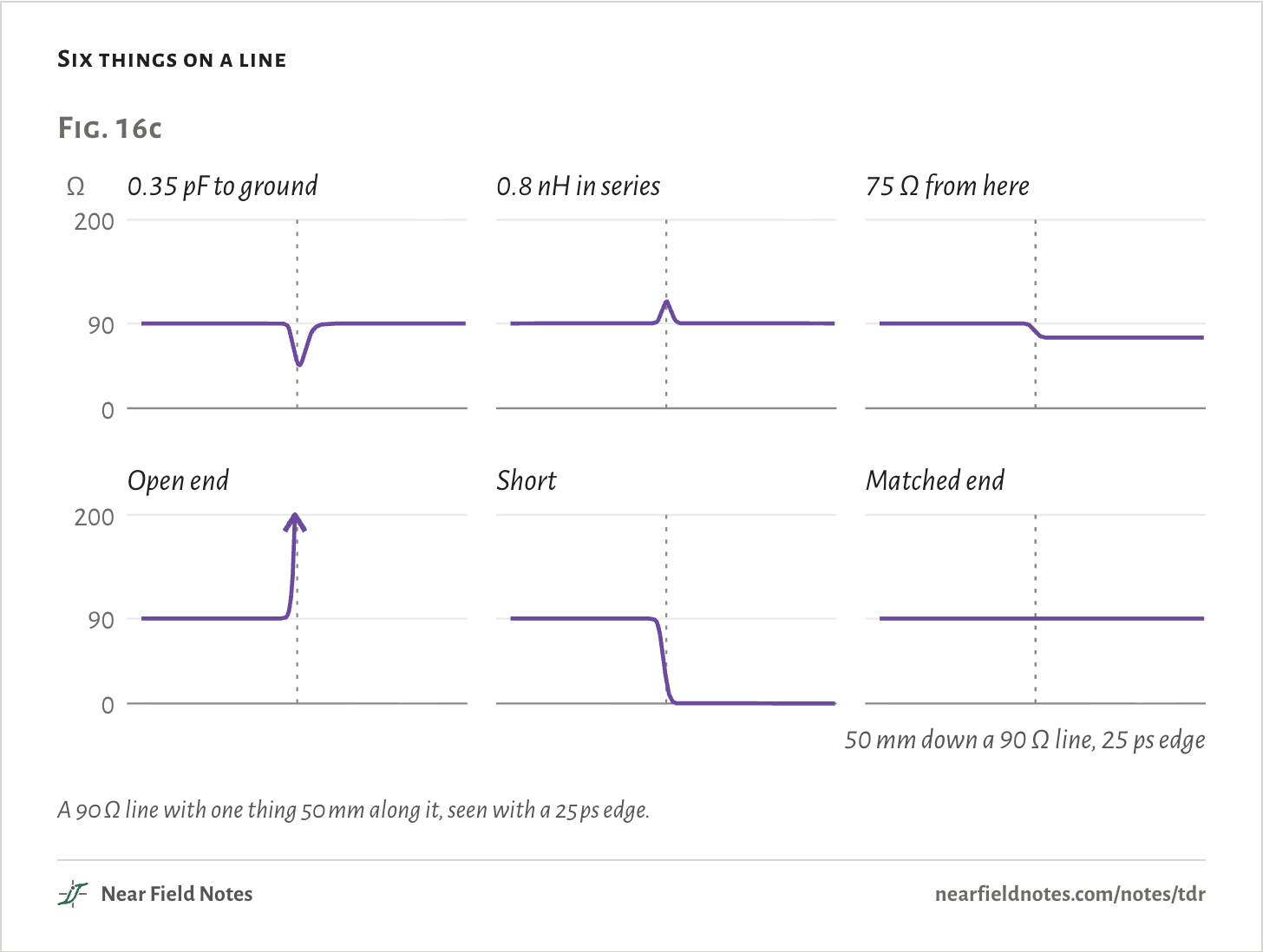
A step that comes back bigger pushes the trace up, a bump. One that comes back smaller pulls it down, a dip. Two shapes do most of the work.

Six things on a line
Fig. 16c0.35 pF to ground0902000.8 nH in series75 Ω from here090200Open endShort090200Matched end50 mm down a 90 Ω line, 25 ps edgeΩFig. 16c0.35 pF to ground0902000.8 nH in series75 Ω from hereOpen end090200ShortMatched end50 mm down a 90 Ω line, 25 ps edgeΩFig. 16c0.35 pF to ground0902000.8 nH in series75 Ω from hereOpen end090200ShortMatched end50 mm down a 90 Ω line, 25 ps edgeΩ
A 90 Ω line with one thing 50 mm along it, seen with a 25 ps edge.
The numbers
Each trace's lowest and highest reading, and where it ends up. The line is 90 Ω.
Thing at 50 mmLowestHighestAfter it
0.35 pF to ground46 Ω90 Ω90 Ω
0.8 nH in series90 Ω113 Ω90 Ω
75 Ω from here75 Ω90 Ω75 Ω
Open end90 ΩOff the topOff the top
Short0 Ω90 Ω0 Ω
Matched end90 Ω90 Ω90 Ω
320

Time is distance

Across is where

Across, the trace is time. An echo goes out and back, so a spot down the line answers after twice its delay:

x=t2τ

=226 ps / (2 × 5.91 ps/mm)=19.1 mmto the first via pair

On this board an echo takes 11.8 ps per mm of trace, there and back. The traces from here on are drawn against mm from the socket pins.

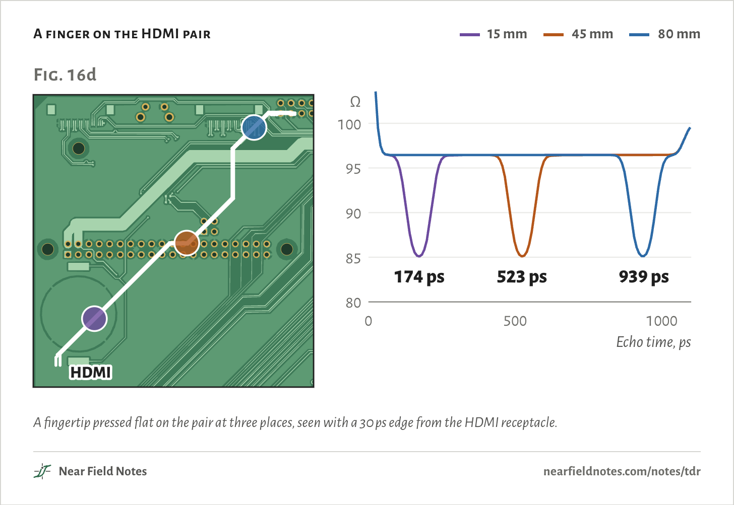
A finger on the HDMI pair
  • 15 mm
  • 45 mm
  • 80 mm
Fig. 16dHDMI8085909510005001000Echo time, psΩ174 ps523 ps939 psFig. 16dHDMI8085909510005001000Echo time, psΩ174 ps523 ps939 psFig. 16dHDMI8085909510005001000Echo time, psΩ174 ps523 ps939 ps
A fingertip pressed flat on the pair at three places, seen with a 30 ps edge from the HDMI receptacle.
The numbers
A fingertip on the 96.5 Ω HDMI pair, seen with a 30 ps edge. 11.74 ps of echo time per mm.
Finger atDip atEcho timeDip reads
15 mm14.8 mm174 ps85 Ω
45 mm44.6 mm523 ps85 Ω
80 mm80 mm939 ps85 Ω
322

The worst spot

The USB-A socket

Back on the USB 3 pair, the deepest feature sits at the socket, ahead of both via pairs.

The socket, close up
  • 15 ps edge
  • 50 ps edge
Fig. 16e2 mm60708090100110−50510mm from the pinsΩ67 Ω103 Ω83 ΩFig. 16e2 mm60708090100110−50510mm from the pinsΩ67 Ω103 Ω83 ΩFig. 16e2 mm60708090100110−50510mm from the pinsΩ67 Ω103 Ω83 Ω
The ground plane just under the top layer. Pale is the hole cut around the pins. The outlined pins carry the pair, which leaves on the top layer.
The numbers
What the TDR reads at the socket, through 60 mm of fixture.
EdgePinsHole past the pins
15 ps67 Ω103 Ω
50 ps83 Ω92 Ω
324

Break it on purpose

Two what-ifs on the same route

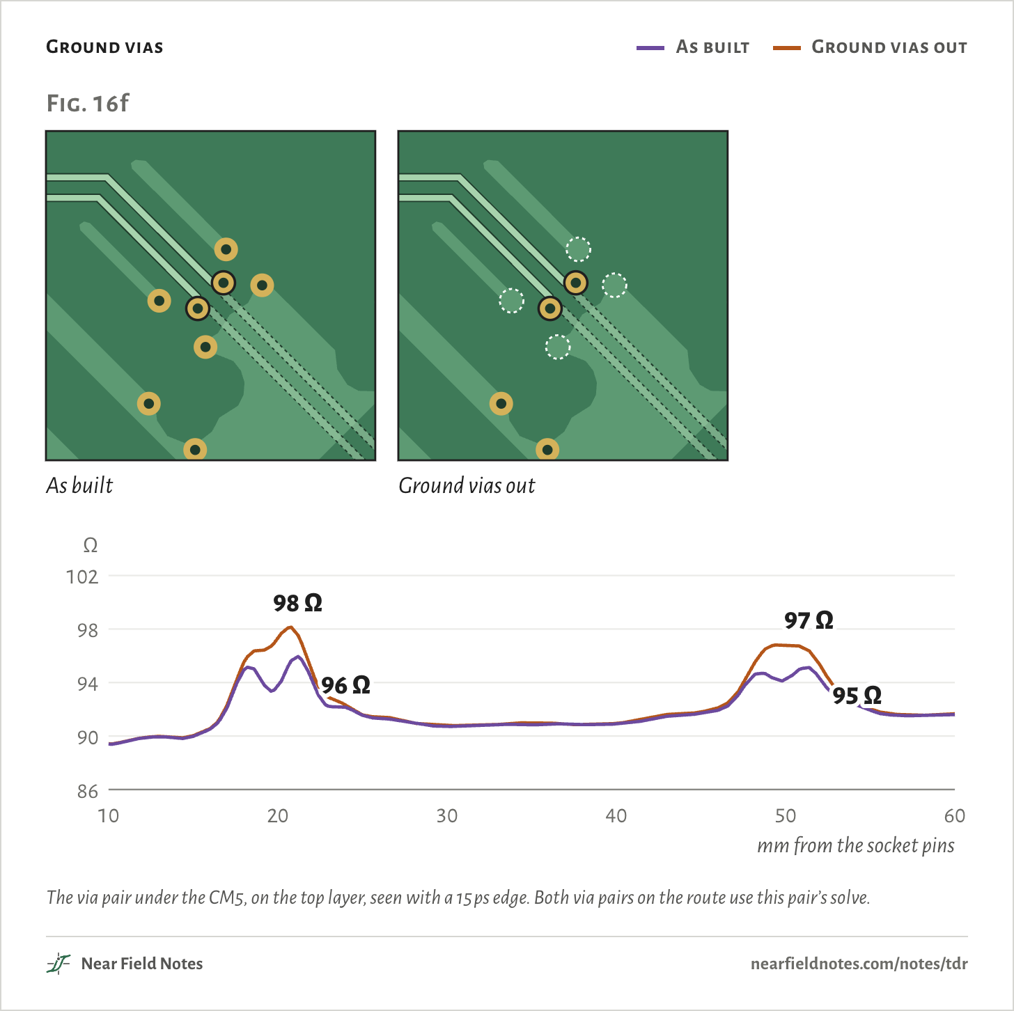
This board’s vias and planes are done right. Taking that away shows what each rule is worth.

Ground vias
  • As built
  • Ground vias out
Fig. 16fAs builtGround vias out86909498102102030405060mm from the socket pinsΩ98 Ω96 Ω97 Ω95 ΩFig. 16fAs builtGround vias out86909498102102030405060mm from the socket pinsΩ98 Ω96 Ω97 Ω95 ΩFig. 16fAs builtGround vias out86909498102102030405060mm from the socket pinsΩ98 Ω96 Ω97 Ω95 Ω
The via pair under the CM5, on the top layer, seen with a 15 ps edge. Both via pairs on the route use this pair’s solve.
The numbers
Highest reading at each via pair with a 15 ps edge.
Via pairAs builtGround vias out
First, 19 mm from the pins96 Ω98 Ω
Second, 49 mm from the pins95 Ω97 Ω
326
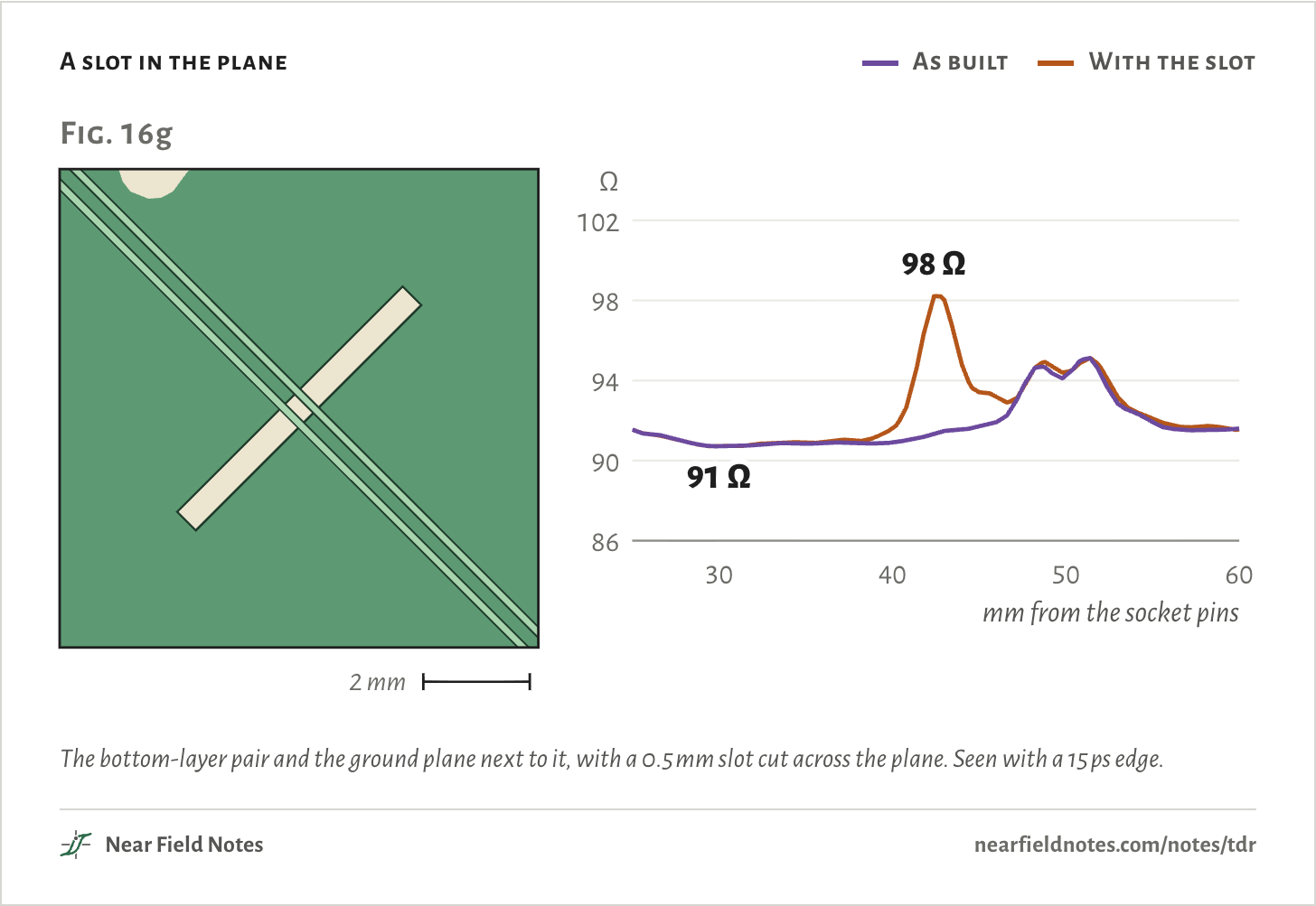
A slot in the plane
  • As built
  • With the slot
Fig. 16g2 mm8690949810230405060mm from the socket pinsΩ98 Ω91 ΩFig. 16g2 mm8690949810230405060mm from the socket pinsΩ98 Ω91 ΩFig. 16g2 mm8690949810230405060mm from the socket pinsΩ98 Ω91 Ω
The bottom-layer pair and the ground plane next to it, with a 0.5 mm slot cut across the plane. Seen with a 15 ps edge.
The numbers
Readings with a 15 ps edge.
PlaceAs builtWith the slot
The slot, 41 mm from the pins91 Ω98 Ω
Plain line, 28 mm91 Ω91 Ω
328

Set the edge yourself

15 to 200 ps, through a fixture or a cable

The edge decides what the trace can see. Features closer than about one edge apart blur into one: at 50 ps that’s 4.2 mm here.

Seen through
15 ps
TDR

15 ps edge

60708090100110020406080mm from the socket pinsΩ67 Ω70 Ω73 Ω78 Ω80 ΩUSB 3.0: 90 ± 15 Ω83 Ω87 Ω89 Ω90 Ω91 Ω82 Ω83 Ω85 Ω87 Ω88 Ω89 Ω91 Ω92 Ω93 Ω94 Ω60708090100110020406080mm from the socket pinsΩ67 Ω70 Ω73 Ω78 Ω80 ΩUSB 3.0: 90 ± 15 Ω83 Ω87 Ω89 Ω90 Ω91 Ω82 Ω83 Ω85 Ω87 Ω88 Ω89 Ω91 Ω92 Ω93 Ω94 Ω60708090100110020406080mm from the socket pinsΩ67 Ω70 Ω73 Ω78 Ω80 ΩUSB 3.0: 90 ± 15 Ω83 Ω87 Ω89 Ω90 Ω91 Ω82 Ω83 Ω85 Ω87 Ω88 Ω89 Ω91 Ω92 Ω93 Ω94 Ω
Socket pins
67 Ω
Highest via
96 Ω
Resolution
1.3 mm
The USB 3 route on the CM5 IO board. Through the fixture at 50 ps, the dashed lines are USB 3.0’s limits for the mated connector, which it sets at that edge.
The numbers
Every edge the control offers. Edges are 20–80%.
EdgePins, fixtureVias, fixturePins, cableVias, cableResolution, fixture
15 ps67 Ω96 Ω82 Ω96 Ω1.3 mm
20 ps70 Ω95 Ω83 Ω96 Ω1.7 mm
25 ps73 Ω95 Ω85 Ω96 Ω2.1 mm
35 ps78 Ω94 Ω87 Ω96 Ω3.0 mm
40 ps80 Ω94 Ω88 Ω96 Ω3.4 mm
50 ps83 Ω94 Ω89 Ω96 Ω4.2 mm
70 ps87 Ω93 Ω91 Ω95 Ω5.9 mm
100 ps89 Ω93 Ω92 Ω95 Ω8.5 mm
131 ps90 Ω93 Ω93 Ω95 Ω11.1 mm
200 ps91 Ω92 Ω94 Ω94 Ω16.9 mm

Fixtures, not cables

What sits in front of the board

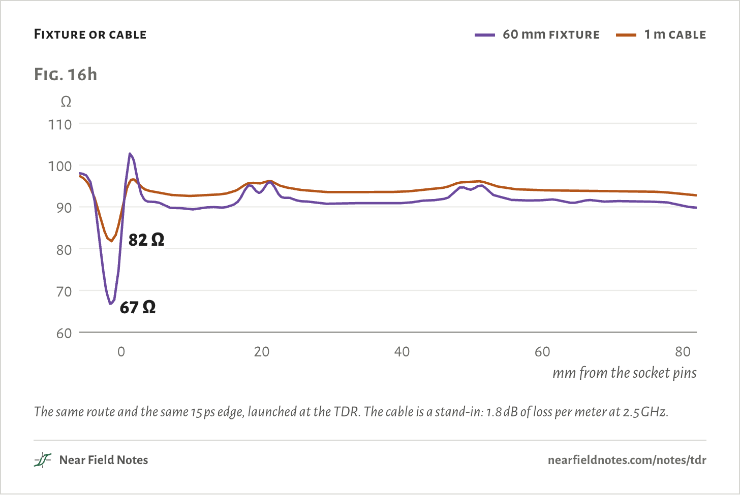
Compliance tests put the board on a short fixture, and the cable shows why.

Fixture or cable
  • 60 mm fixture
  • 1 m cable
Fig. 16h60708090100110020406080mm from the socket pinsΩ67 Ω82 ΩFig. 16h60708090100110020406080mm from the socket pinsΩ67 Ω82 ΩFig. 16h60708090100110020406080mm from the socket pinsΩ67 Ω82 Ω
The same route and the same 15 ps edge, launched at the TDR. The cable is a stand-in: 1.8 dB of loss per meter at 2.5 GHz.
The numbers
A 15 ps edge launched at the TDR.
PlaceThrough the fixtureThrough 1 m of cable
Socket pins67 Ω82 Ω
Hole past the pins103 Ω97 Ω
First via pair96 Ω96 Ω
Second via pair95 Ω96 Ω
330

What the specs ask for

Each one names its edge

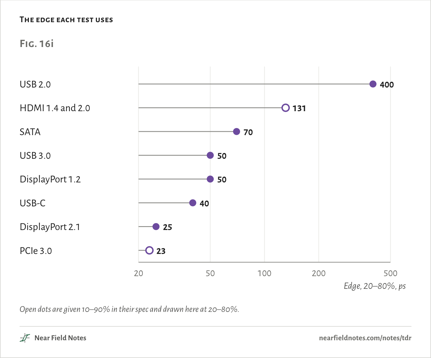
Many fast standards check impedance with a TDR, and each one that does fixes the edge. Faster links care about smaller features, so they test with sharper edges.

The edge each test uses
Fig. 16i2050100200500USB 2.0400HDMI 1.4 and 2.0131SATA70USB 3.050DisplayPort 1.250USB-C40DisplayPort 2.125PCIe 3.023Edge, 20–80%, psFig. 16i2050100200500USB 2.0400HDMI 1.4 and 2.0131SATA70USB 3.050DisplayPort 1.250USB-C40DisplayPort 2.125PCIe 3.023Edge, 20–80%, psFig. 16i2050100200500USB 2.0400HDMI 1.4 and 2.0131SATA70USB 3.050DisplayPort 1.250USB-C40DisplayPort 2.125PCIe 3.023Edge, 20–80%, ps
Open dots are given 10–90% in their spec and drawn here at 20–80%.
The numbers
Open dots are converted from a 10–90% edge: for a smooth edge, 10–90% is 1.52 times 20–80%.
StandardWhat is testedEdge, 20–80%As the spec gives it
USB 2.0Pair in a USB-C cable400 ps400 ps
HDMI 1.4 and 2.0Cable131 ps200 ps, 10–90%
SATACable and connector70 ps70 ps
USB 3.0Mated connector50 ps50 ps
DisplayPort 1.2Cable50 ps50 ps
USB-CMated connector40 ps40 ps
DisplayPort 2.1DP80 cable25 ps25 ps
PCIe 3.0Board traces23 ps35 ps, 10–90%
332

No TDR? A VNA

The same echoes, against frequency

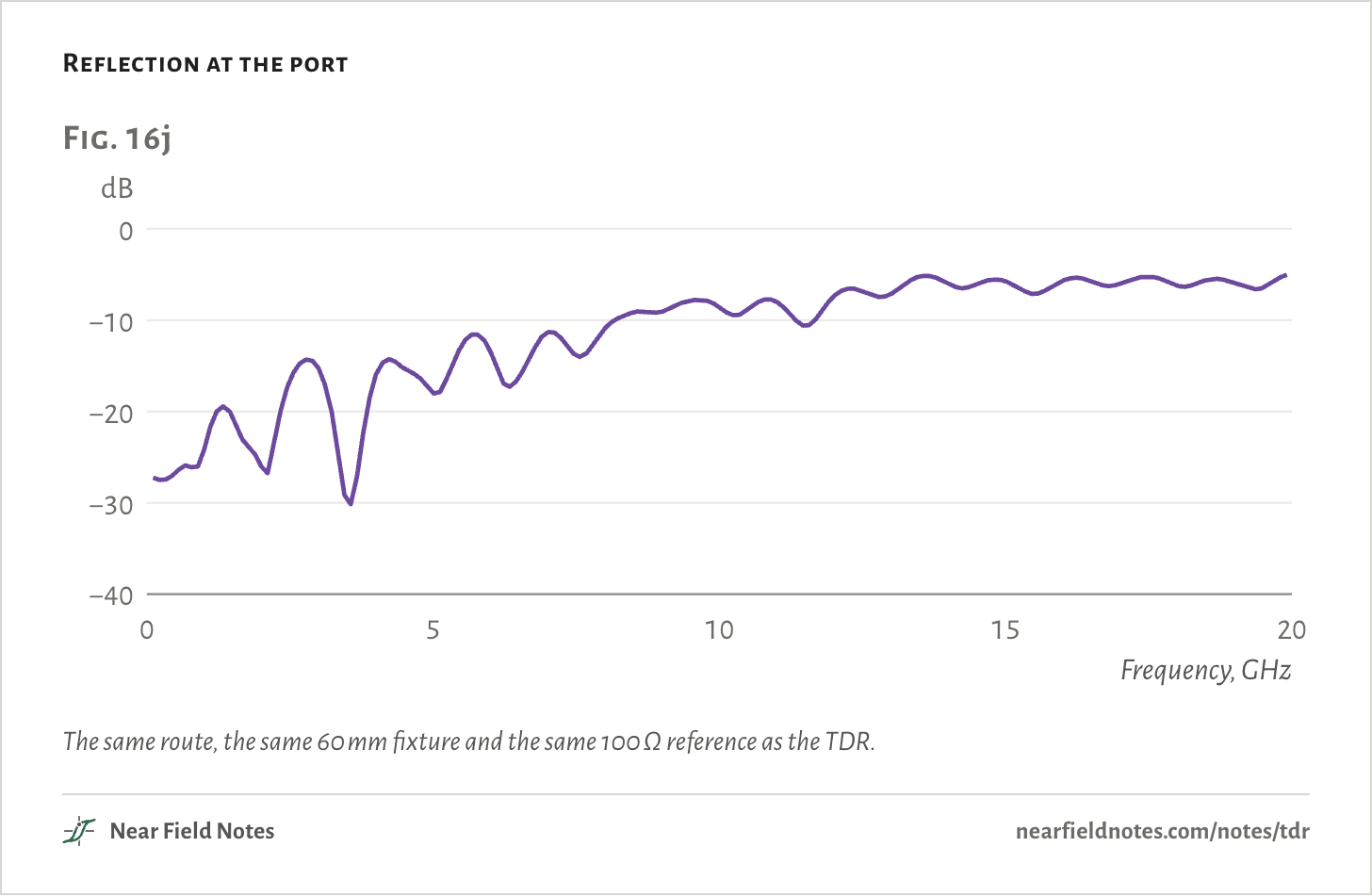
A network analyzer measures the same reflections, one frequency at a time.

Reflection at the port
Fig. 16j−40−30−20−10005101520Frequency, GHzdBFig. 16j−40−30−20−10005101520Frequency, GHzdBFig. 16j−40−30−20−10005101520Frequency, GHzdB
The same route, the same 60 mm fixture and the same 100 Ω reference as the TDR.
The numbers
Reflection at the TDR's port, 100 Ω reference, through 60 mm of fixture.
FrequencyReflection
1 GHz−24.2 dB
2.5 GHz−17.3 dB
5 GHz−18.0 dB
10 GHz−8.6 dB
15 GHz−5.8 dB
20 GHz−5.0 dB
334

Key to TDR traces

What is this bump?

  1. 1aThe trace dipsGo to 2
  2. 1bThe trace climbsGo to 3
  3. 2aIt comes back to the lineExtra capacitance: pads, pins, a stub
  4. 2bIt steps down and staysA lower-impedance line from there on
  5. 2cIt drops to zeroA short
  6. 3aIt comes back to the lineExtra inductance or a broken return path
  7. 3bIt steps up and staysA higher-impedance line from there on
  8. 3cIt shoots off the topAn open end

To find where: echo time ÷ 11.8 ps is mm of trace on this board.

Conditions

Board
Raspberry Pi CM5 IO board, revision 2, from its KiCad files. 4 layers, 1.6 mm: top, 0.09 mm, ground, 1.28 mm, ground, 0.09 mm, bottom. FR-4, εr 4.5.
Route
USB 3 receive pair, 0.147 mm traces with a 0.253 mm gap. 76.45 mm from the socket pins to the module.
Lines
90.1 Ω and 5.91 ps/mm from a 2D cross-section with solder mask. The HDMI pair is 96.5 Ω.
Pieces
The socket’s footprint, the via pair under the CM5 with and without its ground vias, and the slot, each solved in 3D from the board’s copper. The slot sits 41 mm from the pins, where its window lies on the bottom-layer run.
Stand-ins
Fixture 60 mm at 90 Ω. Cable 1 m at 90 Ω with 1.8 dB/m at 2.5 GHz. Plug and socket contacts 20 mm at 98 Ω. Module 6 mm at 88 Ω into a 90 Ω receiver.
TDR
100 Ω differential source, a smooth edge, rise times 20–80%
Finger
A 2D cross-section: 0.25 mm of dry skin over tissue, through the mask, pressed flat over 6 mm. It reads 12% low. A 3D solve of a fingertip on the same pair dips 15%.
Solver
openEMS v0.37 for the pieces, chained into the lines in the frequency domain. Copper has skin loss and FR-4 a loss tangent of 0.02.

Simulated only. Nothing on this page has been measured on a board yet.

Limits

  • The cable, the plug in the socket and the module have no design files. They set the trace left of the pins and past 76 mm.
  • Both via pairs use the solve of the one under the CM5. The socket-side pair has its own ground vias and may read a little differently.
  • Each piece was driven from one side. Its reflection from the other side is mirrored from the first, which holds for small reflections like these.
  • The pieces were solved to 40 GHz. At 40 GHz a 15 ps edge still has 8% of its low-frequency strength, so 15 ps readings are the least sure.

Files

  • tdrsim/route.pyThe route, pieced together
  • tdrsim/line_fd.pyThe line solver and the TDR
  • runs/field/The 3D pieces
  • runs/layout/cm5io.jsonThe board’s copper, read from KiCad
  • docs/spec_tdr.mdEvery spec’s TDR test, with its source

Sources

Like this note?

Rev 1 ·
  1. Rev 1First published

Each fix gets a line here, with the reader's name if they want credit.

Did it answer your question?

Want more on this?

Report a problem

What should the next note be? Ask for one