Near Field Notes

Note 1Signal integrityRev 1Watch the video · 0:12

Ground cut

Should you cut ground under connector pads?

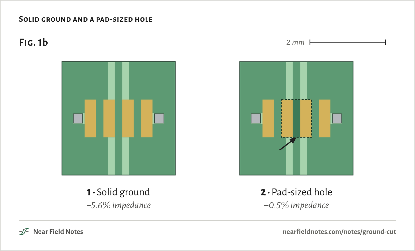
Yes, on high-speed pairs whose pads are wider than their traces. A hole the size of the pads takes USB-C’s 6% impedance dip to 0.5%, and one 0.2 mm bigger overshoots by 6%.

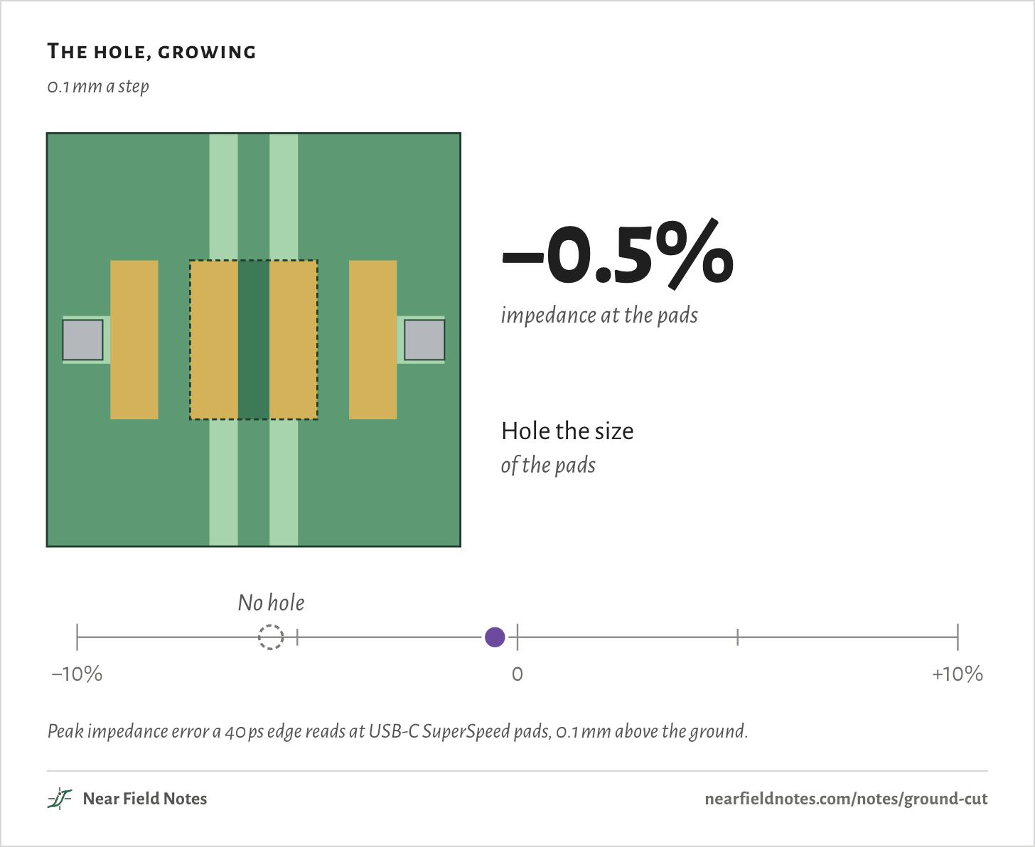
The hole, growing

0.1 mm a step

−5.6%No hole−5.1%Hole 0.2 mm smallerthan the pads−3.6%Hole 0.1 mm smallerthan the pads−0.5%Hole the sizeof the pads+2.7%Hole 0.1 mm biggerthan the pads+5.8%Hole 0.2 mm biggerthan the pads+7.5%Hole 0.3 mm biggerthan the padsimpedance at the pads−10%0+10%No hole−5.6%No hole−5.1%Hole 0.2 mm smallerthan the pads−3.6%Hole 0.1 mm smallerthan the pads−0.5%Hole the sizeof the pads+2.7%Hole 0.1 mm biggerthan the pads+5.8%Hole 0.2 mm biggerthan the pads+7.5%Hole 0.3 mm biggerthan the padsimpedance at the pads−10%0+10%No hole−5.6%No hole−5.1%Hole 0.2 mm smallerthan the pads−3.6%Hole 0.1 mm smallerthan the pads−0.5%Hole the sizeof the pads+2.7%Hole 0.1 mm biggerthan the pads+5.8%Hole 0.2 mm biggerthan the pads+7.5%Hole 0.3 mm biggerthan the padsimpedance at the pads−10%0+10%No hole

Peak impedance error a 40 ps edge reads at USB-C SuperSpeed pads, 0.1 mm above the ground.

What a ground cut is

USB-C pads on a JLCPCB 4-layer board

A hole in the ground layer, right under a connector’s pads. It’s a signal integrity fix for high-speed pairs, like USB-C’s 10 Gbit/s SuperSpeed lines and HDMI. The pads are wider than their traces, so over solid ground they add capacitance and the impedance dips. At these speeds a dip bounces part of the signal back. Through the hole the pads see ground farther down, and the impedance holds.

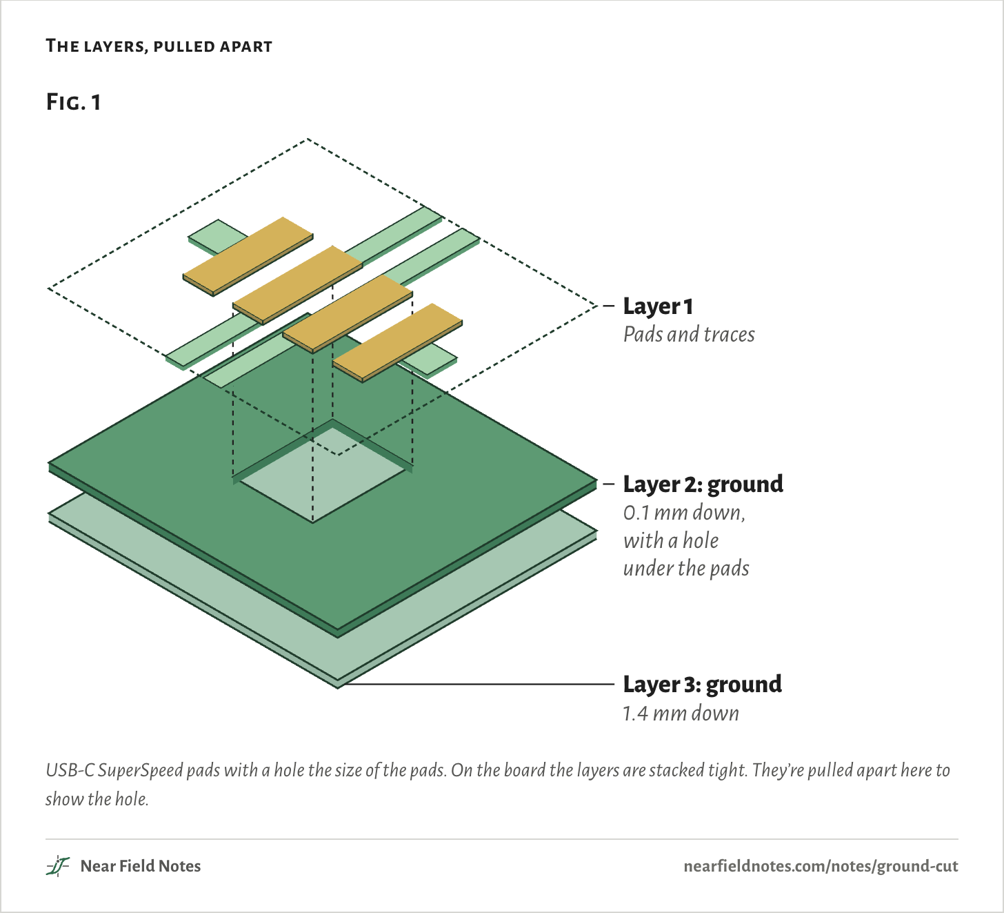
The layers, pulled apart
Fig. 1Layer 1Pads and tracesLayer 2: ground0.1 mm down,with a holeunder the padsLayer 3: ground1.4 mm downFig. 1Layer 1Pads and tracesLayer 2: ground0.1 mm down,with a holeunder the padsLayer 3: ground1.4 mm downFig. 1Layer 1Pads and tracesLayer 2: ground0.1 mm down,with a holeunder the padsLayer 3: ground1.4 mm down

USB-C SuperSpeed pads with a hole the size of the pads. On the board the layers are stacked tight. They’re pulled apart here to show the hole.

Solid ground and a pad-sized hole
Fig. 1b2 mm1 · Solid ground−5.6% impedance2 · Pad-sized hole−0.5% impedanceFig. 1b2 mm1 · Solid ground−5.6% impedance2 · Pad-sized hole−0.5% impedanceFig. 1b2 mm1 · Solid ground−5.6% impedance2 · Pad-sized hole−0.5% impedance
24

Key to ground cut

Do these pads need a hole in the ground?

  1. 1aPads less than 0.05 mm wider than their tracesNo hole
  2. 1bPads 0.05 mm or more widerGo to 2
  3. 2aConnector or choke padsA hole the size of the pads
  4. 2bA series 0402 or 0201 capacitorA hole under the part, 0.1 mm bigger

With the ground 0.1 mm down, the traces are 0.17 to 0.21 mm wide. With it 0.2 mm down they are 0.32 to 0.41 mm, as wide as most pads.

Size the hole yourself

5 footprints, 2 ground depths
Footprint
Ground below the pads
None
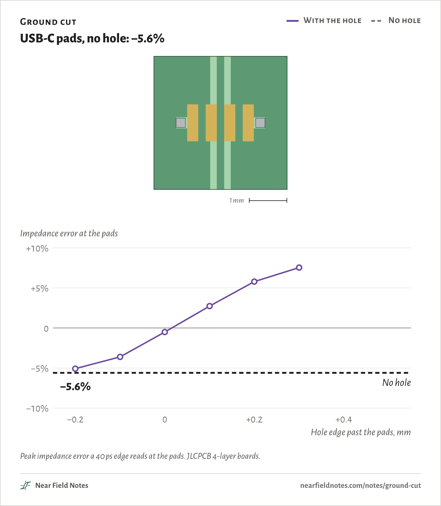
Ground cut

USB-C pads, no hole: −5.6%

  • With the hole
  • No hole
−15%−10%−5%0+5%+10%−0.20+0.2+0.4Hole edge past the pads, mmImpedance error at the padsNo hole−5.6%−5.1%−3.6%−0.5%+2.7%+5.8%+7.5%−15%−10%−5%0+5%+10%−0.20+0.2+0.4Hole edge past the pads, mmImpedance error at the padsNo hole−0.3%−0.2%+0.2%+1.0%+2.2%+3.6%+4.7%−30%−20%−10%0+10%+20%−0.20+0.2+0.4Hole edge past the pads, mmImpedance error at the padsNo hole−11.9%−9.9%−4.8%+1.6%+9.2%+15.8%+19.6%−30%−20%−10%0+10%+20%−0.20+0.2+0.4Hole edge past the pads, mmImpedance error at the padsNo hole−1.5%−0.3%+1.4%+4.0%+7.5%+10.5%+12.8%−40%−30%−20%−10%0+10%+20%−0.20+0.2+0.4Hole edge past the pads, mmImpedance error at the padsNo hole−20.8%−19.3%−15.2%−9.0%−1.1%+5.5%+9.5%+13.1%+16.6%−40%−30%−20%−10%0+10%+20%−0.20+0.2+0.4Hole edge past the pads, mmImpedance error at the padsNo hole−9.6%−9.1%−7.2%−4.5%−0.8%+2.7%+5.2%+7.5%+9.6%−15%−10%−5%0+5%+10%+15%+20%−0.20+0.2+0.4Hole edge past the pads, mmImpedance error at the padsNo hole−9.8%−8.7%−4.1%+2.3%+6.9%+10.1%+13.1%+15.9%−15%−10%−5%0+5%+10%+15%+20%−0.20+0.2+0.4Hole edge past the pads, mmImpedance error at the padsNo hole−2.5%−2.1%−0.6%+1.8%+4.0%+5.7%+7.3%+8.8%−30%−20%−10%0+10%+20%+30%+40%−0.20+0.2+0.4Hole edge past the pads, mmImpedance error at the padsNo hole−13.9%−12.0%−4.2%+8.2%+18.4%+24.9%+32.2%+35.7%−30%−20%−10%0+10%+20%+30%+40%−0.20+0.2+0.4Hole edge past the pads, mmImpedance error at the padsNo hole−0.5%+0.2%+3.3%+8.1%+13.2%+16.9%+21.4%+23.6%−10%−5%0+5%+10%−0.20+0.2+0.4Hole edge past the pads, mmImpedance error at the padsNo hole−5.6%−5.1%−3.6%−0.5%+2.7%+5.8%+7.5%−10%−5%0+5%+10%−0.20+0.2+0.4Hole edge past the pads, mmImpedance error at the padsNo hole−0.3%−0.2%+0.2%+1.0%+2.2%+3.6%+4.7%−20%−10%0+10%+20%−0.20+0.2+0.4Hole edge past the pads, mmImpedance error at the padsNo hole−11.9%−9.9%−4.8%+1.6%+9.2%+15.8%+19.6%−20%−10%0+10%+20%−0.20+0.2+0.4Hole edge past the pads, mmImpedance error at the padsNo hole−1.5%−0.3%+1.4%+4.0%+7.5%+10.5%+12.8%−30%−20%−10%0+10%+20%−0.20+0.2+0.4Hole edge past the pads, mmImpedance error at the padsNo hole−20.8%−19.3%−15.2%−9.0%−1.1%+5.5%+9.5%+13.1%+16.6%−30%−20%−10%0+10%+20%−0.20+0.2+0.4Hole edge past the pads, mmImpedance error at the padsNo hole−9.6%−9.1%−7.2%−4.5%−0.8%+2.7%+5.2%+7.5%+9.6%−15%−10%−5%0+5%+10%+15%+20%−0.20+0.2+0.4Hole edge past the pads, mmImpedance error at the padsNo hole−9.8%−8.7%−4.1%+2.3%+6.9%+10.1%+13.1%+15.9%−15%−10%−5%0+5%+10%+15%+20%−0.20+0.2+0.4Hole edge past the pads, mmImpedance error at the padsNo hole−2.5%−2.1%−0.6%+1.8%+4.0%+5.7%+7.3%+8.8%−30%−20%−10%0+10%+20%+30%+40%−0.20+0.2+0.4Hole edge past the pads, mmImpedance error at the padsNo hole−13.9%−12.0%−4.2%+8.2%+18.4%+24.9%+32.2%+35.7%−30%−20%−10%0+10%+20%+30%+40%−0.20+0.2+0.4Hole edge past the pads, mmImpedance error at the padsNo hole−0.5%+0.2%+3.3%+8.1%+13.2%+16.9%+21.4%+23.6%−10%−5%0+5%+10%−0.20+0.2+0.4Hole edge past the pads, mmImpedance error at the padsNo hole−5.6%−5.1%−3.6%−0.5%+2.7%+5.8%+7.5%−10%−5%0+5%+10%−0.20+0.2+0.4Hole edge past the pads, mmImpedance error at the padsNo hole−0.3%−0.2%+0.2%+1.0%+2.2%+3.6%+4.7%−20%−10%0+10%+20%−0.20+0.2+0.4Hole edge past the pads, mmImpedance error at the padsNo hole−11.9%−9.9%−4.8%+1.6%+9.2%+15.8%+19.6%−20%−10%0+10%+20%−0.20+0.2+0.4Hole edge past the pads, mmImpedance error at the padsNo hole−1.5%−0.3%+1.4%+4.0%+7.5%+10.5%+12.8%−30%−20%−10%0+10%+20%−0.20+0.2+0.4Hole edge past the pads, mmImpedance error at the padsNo hole−20.8%−19.3%−15.2%−9.0%−1.1%+5.5%+9.5%+13.1%+16.6%−30%−20%−10%0+10%+20%−0.20+0.2+0.4Hole edge past the pads, mmImpedance error at the padsNo hole−9.6%−9.1%−7.2%−4.5%−0.8%+2.7%+5.2%+7.5%+9.6%−15%−10%−5%0+5%+10%+15%+20%−0.20+0.2+0.4Hole edge past the pads, mmImpedance error at the padsNo hole−9.8%−8.7%−4.1%+2.3%+6.9%+10.1%+13.1%+15.9%−15%−10%−5%0+5%+10%+15%+20%−0.20+0.2+0.4Hole edge past the pads, mmImpedance error at the padsNo hole−2.5%−2.1%−0.6%+1.8%+4.0%+5.7%+7.3%+8.8%−30%−20%−10%0+10%+20%+30%+40%−0.20+0.2+0.4Hole edge past the pads, mmImpedance error at the padsNo hole−13.9%−12.0%−4.2%+8.2%+18.4%+24.9%+32.2%+35.7%−30%−20%−10%0+10%+20%+30%+40%−0.20+0.2+0.4Hole edge past the pads, mmImpedance error at the padsNo hole−0.5%+0.2%+3.3%+8.1%+13.2%+16.9%+21.4%+23.6%

Peak impedance error a 40 ps edge reads at the pads. JLCPCB 4-layer boards.

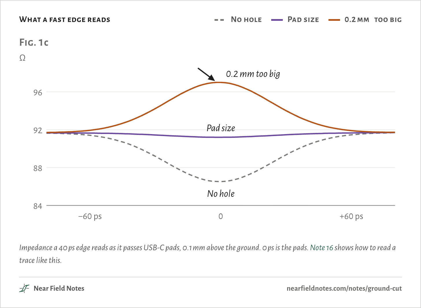
What a fast edge reads
  • No hole
  • Pad size
  • 0.2 mm too big
Fig. 1cΩ84889296−60 ps0+60 psNo hole0.2 mm too bigPad sizeFig. 1cΩ84889296−60 ps0+60 psNo hole0.2 mm too bigPad sizeFig. 1cΩ84889296−60 ps0+60 psNo hole0.2 mm too bigPad size

Impedance a 40 ps edge reads as it passes USB-C pads, 0.1 mm above the ground. 0 ps is the pads. Note 16 shows how to read a trace like this.

26

Conditions

Footprints
USB-C SuperSpeed pads 0.30 by 1.00 mm on a 0.5 mm pitch. HDMI and DisplayPort pads 0.30 by 1.90 mm. 0402 and 0201 capacitors on KiCad’s pads. 0805 choke pads.
Board
JLCPCB 4-layer, 1.6 mm: JLC04161H-3313 with the ground 0.10 mm down, JLC04161H-7628 with it 0.21 mm down
Route
90 Ω differential, 100 Ω for HDMI, widths from a 2D field solver
Hole
In the layer-2 ground, with layer 3 solid below it
Measure
Peak impedance a 40 ps edge reads at the footprint, against the line’s own
Solver
openEMS, 327 runs in all. Copper is a perfect conductor and the laminate has no loss.
Check
A finer mesh moves the USB-C results by 0.2% or less

Simulated only. Nothing on this page has been measured on a board yet.

Limits

  • Pads only. The connector’s pins and shell, and the vias around them, aren’t in the model.
  • ESD diodes add 3 to 7 times a pad’s capacitance. A hole 3 mm long takes a 0.2 pF diode’s dip from 17% to 6%, and a 0.5 pF diode’s only from 34% to 29%.
  • Noise on both lines together leaks into the gap between layers 2 and 3, 0.1 to 0.9% of it below 10 GHz with a hole 0.1 mm past the pads. Under 0.1% radiates. Keep the hole centered under the pair.

Files

  • padsim/geom.pyEvery footprint and hole, as the solver saw them
  • runs/results.jsonAll 327 runs

Sources

Like this note?

Rev 1 ·
  1. Rev 1First published

Each fix gets a line here, with the reader's name if they want credit.

Did it answer your question?

Want more on this?

Report a problem

What should the next note be? Ask for one