Near Field Notes

Note 17Signal integrityRev 1Watch the video · 0:09

Via stubs

How long a via stub can a fast link take?

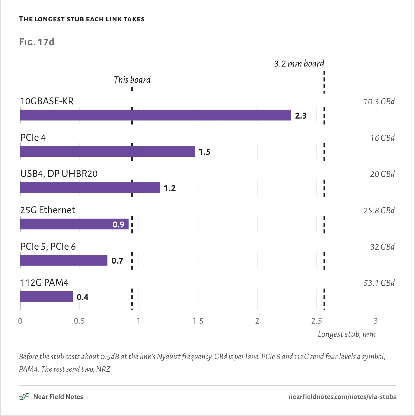
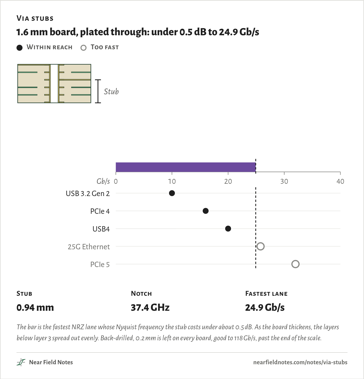
About 23.6 mm divided by the lane’s rate in GBd: 2.3 mm for 10GBASE-KR, 0.7 mm for PCIe 5. Past that, the stub costs more than about 0.5 dB at the link’s Nyquist frequency. A via to layer 3 of a 1.6 mm board leaves 0.94 mm, fine to about 25 Gb/s.

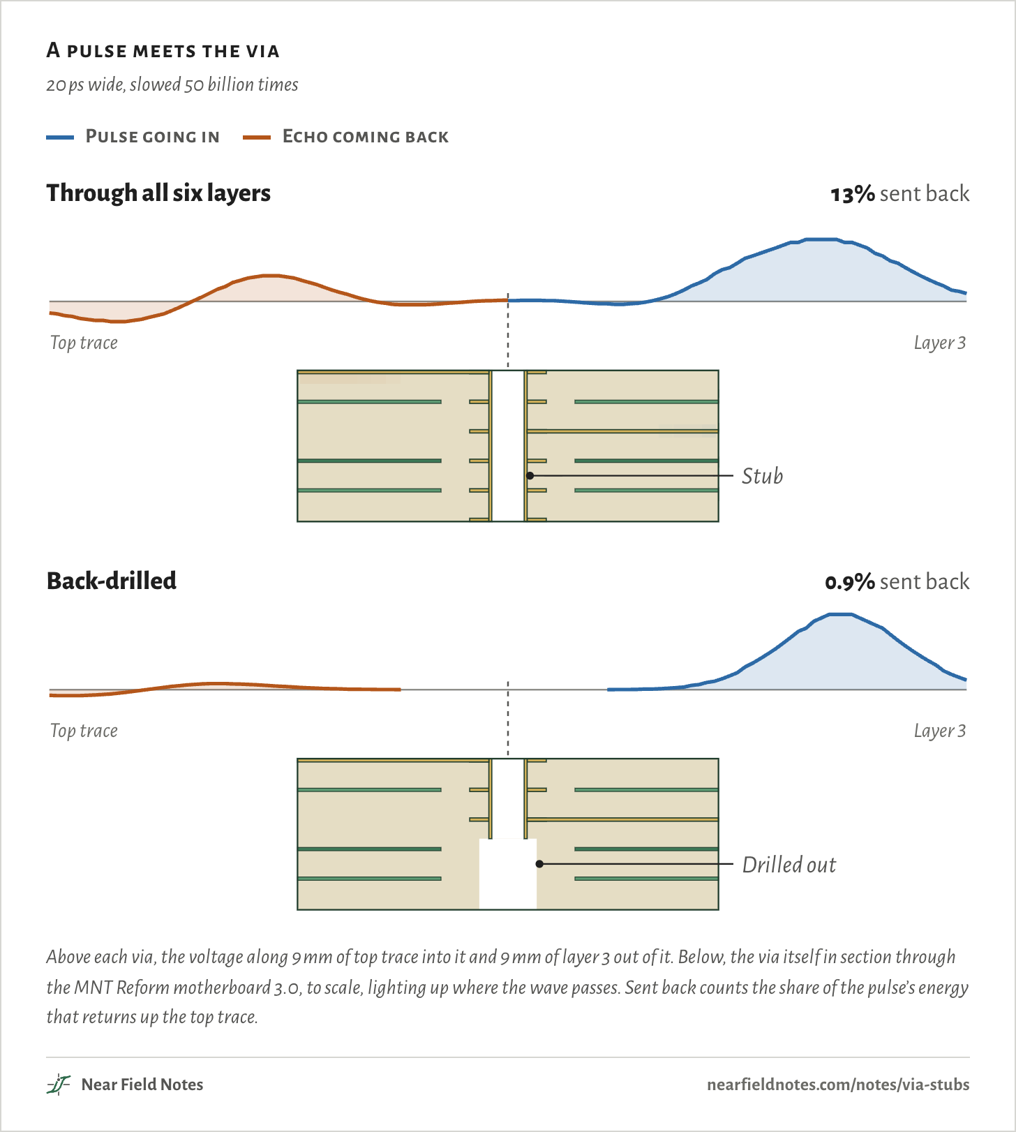
The figure sends one fast pulse into two vias that drop from the top layer to layer 3. In the first, the plated barrel runs on to the bottom of the board. That leftover length, the stub, rings and sends 13% of the pulse back.

In the second, a drill has cut the stub away from below. Only 0.9% comes back.

A pulse meets the via

20 ps wide, slowed 50 billion times

  • Pulse going in
  • Echo coming back
Through all six layers13% sent backTop traceLayer 3StubBack-drilled0.9% sent backTop traceLayer 3Drilled outThrough all six layers13% sent backTop traceLayer 3StubBack-drilled0.9% sent backTop traceLayer 3Drilled outThrough all six layers13% sent backTop traceLayer 3StubBack-drilled0.9% sent backTop traceLayer 3Drilled out
Above each via, the voltage along 9 mm of top trace into it and 9 mm of layer 3 out of it. Below, the via itself in section through the MNT Reform motherboard 3.0, to scale, lighting up where the wave passes. Sent back counts the share of the pulse’s energy that returns up the top trace.
The numbers
ViaEnergy sent backEnergy throughStubDown the stub and backPeak on layer 3
Through all six layers13%87%0.94 mm13.4 ps0.82 V
Back-drilled0.9%99%0.2 mm2.8 ps0.99 V

What a via stub is

One via on the MNT Reform motherboard 3.0

A via carries a signal from one layer to another through a plated hole. Drilled straight through the board, its barrel runs from the top layer to the bottom, whichever layers the signal uses.

When the signal leaves on an inner layer, the barrel below it carries nothing on. That leftover length is the stub. It hangs off the line like a short wire with an open end. A TDR sees it as a dip, as Note 16 shows.

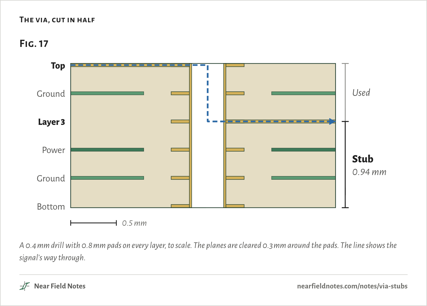
On a 1.6 mm, 6-layer board, a via from the top layer to layer 3 leaves 0.94 mm of stub.

The via, cut in half
Fig. 17TopGroundLayer 3PowerGroundBottomUsedStub0.94 mm0.5 mmFig. 17TopGroundLayer 3PowerGroundBottomUsedStub0.94 mm0.5 mmFig. 17TopGroundLayer 3PowerGroundBottomUsedStub0.94 mm0.5 mm
A 0.4 mm drill with 0.8 mm pads on every layer, to scale. The planes are cleared 0.3 mm around the pads. The line shows the signal’s way through.
The numbers
LayerWhat it isDepth of its center
F.CuTop0.018 mm
In1Ground0.327 mm
In2Layer 30.635 mm
In3Power0.945 mm
In4Ground1.254 mm
B.CuBottom1.562 mm
StubBarrel below layer 30.94 mm

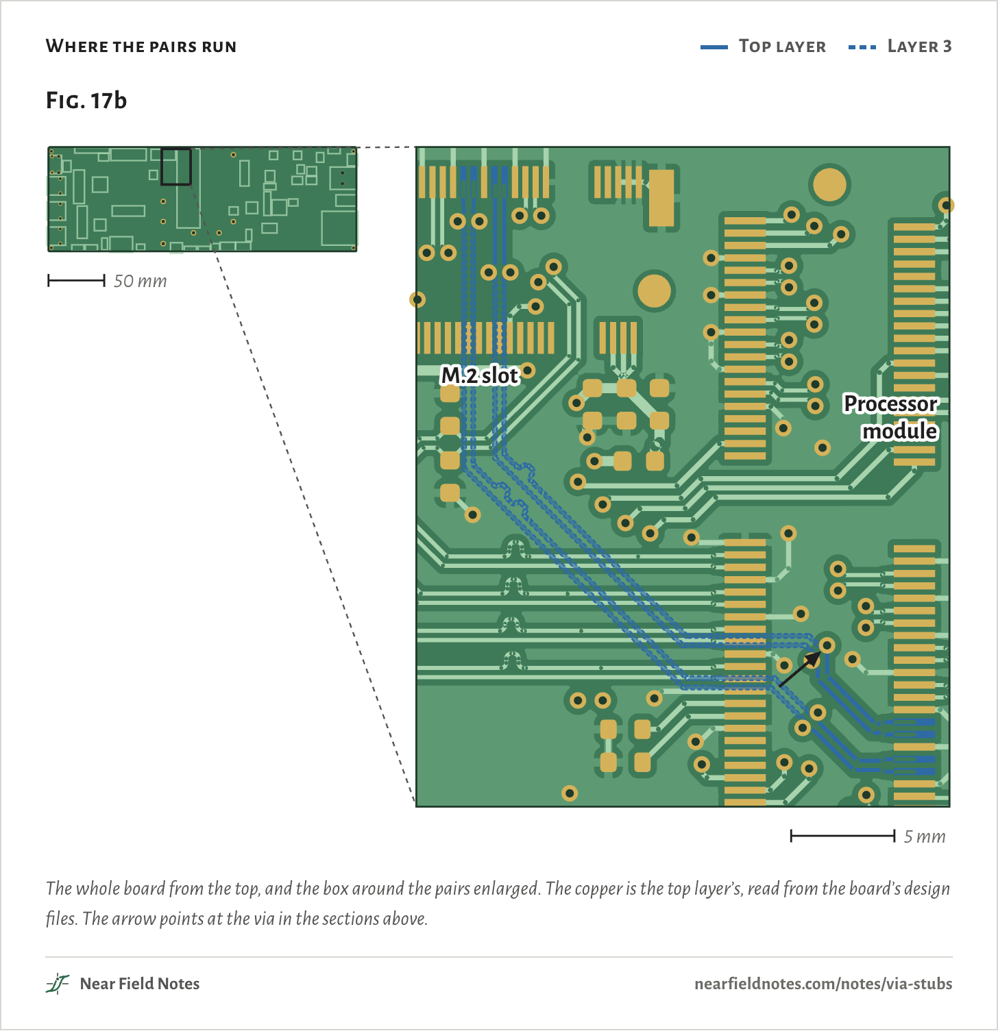
The MNT Reform laptop’s motherboard has vias like this on its PCIe lines. The processor module reaches the M.2 slot over two pairs, one each way.

Each pair leaves the module’s socket on short top-layer traces, drops to layer 3 and comes back up at the slot. All eight vias are plated through all six layers, so each one carries a 0.94 mm stub.

Where the pairs run
  • Top layer
  • Layer 3
Fig. 17b50 mmM.2 slotProcessormodule5 mmFig. 17b50 mmM.2 slotProcessormodule5 mmFig. 17b50 mmM.2 slotProcessormodule5 mm
The whole board from the top, and the box around the pairs enlarged. The copper is the top layer’s, read from the board’s design files. The arrow points at the via in the sections above.
The numbers
Pair, lineEndDrillPadPlated
PCIe RX NM.2 slot0.4 mm0.8 mmF.Cu to B.Cu
PCIe RX PM.2 slot0.4 mm0.8 mmF.Cu to B.Cu
PCIe TX NM.2 slot0.4 mm0.8 mmF.Cu to B.Cu
PCIe TX PM.2 slot0.4 mm0.8 mmF.Cu to B.Cu
PCIe RX NProcessor module0.4 mm0.8 mmF.Cu to B.Cu
PCIe RX PProcessor module0.4 mm0.8 mmF.Cu to B.Cu
PCIe TX NProcessor module0.4 mm0.8 mmF.Cu to B.Cu
PCIe TX PProcessor module0.4 mm0.8 mmF.Cu to B.Cu

A quarter-wave notch

Three stubs, swept to 60 GHz

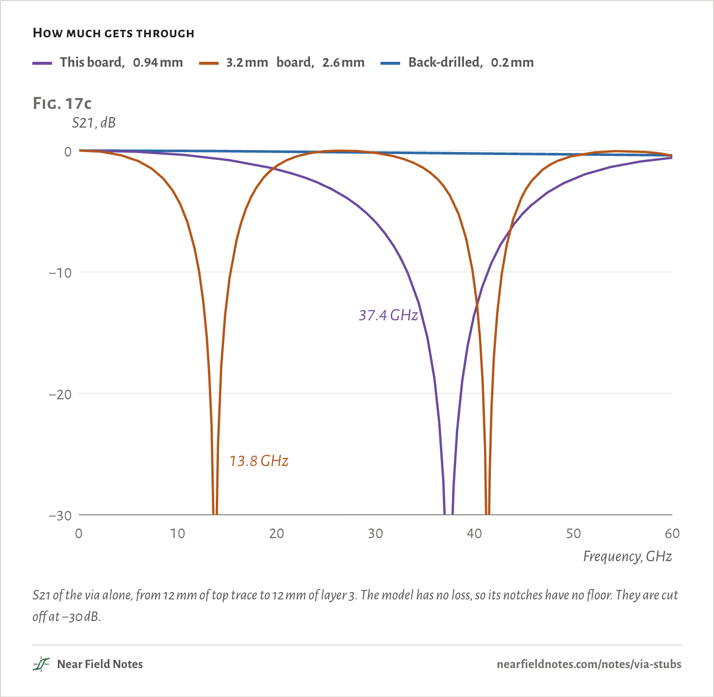
An edge that runs down the stub bounces off its open end and comes back up. At the frequency where the stub is a quarter wave long, the bounce arrives back exactly out of step. The open end then looks like a short at the junction, and almost nothing gets past.

fnotch=c4Lεr

=300 mm/ns4 × 0.945 mm × 2.12=37.4 GHz

So the notch falls as one over the stub’s length. In FR-4 it sits near 35 GHz divided by the stub in mm.

How much gets through
  • This board, 0.94 mm
  • 3.2 mm board, 2.6 mm
  • Back-drilled, 0.2 mm
Fig. 17cS21, dB0−10−20−300102030405060Frequency, GHz37.4 GHz13.8 GHzFig. 17cS21, dB0−10−20−300102030405060Frequency, GHz37.4 GHz13.8 GHzFig. 17cS21, dB0−10−20−300102030405060Frequency, GHz37.4 GHz13.8 GHz
S21 of the via alone, from 12 mm of top trace to 12 mm of layer 3. The model has no loss, so its notches have no floor. They are cut off at −30 dB.
The numbers
S21 atBack-drilledThis boardThick board
Stub0.2 mm0.94 mm2.6 mm
5 GHz−0.01 dB−0.08 dB−0.56 dB
10 GHz−0.03 dB−0.32 dB−4.00 dB
12.5 GHz−0.04 dB−0.51 dB−11.85 dB
16 GHz−0.06 dB−0.89 dB−7.22 dB
20 GHz−0.09 dB−1.54 dB−1.27 dB
28 GHz−0.16 dB−4.42 dB−0.04 dB
37.4 GHz−0.24 dB−56.73 dB−3.55 dB
50 GHz−0.33 dB−2.32 dB−0.43 dB
Notch176.7 GHz37.4 GHz13.8 GHz
338

Long before the notch

The longest stub for six links

A link never runs at the notch. What matters is its Nyquist frequency, half its baud rate: the tone of its fastest pattern, 1010. That is where a channel’s loss is usually judged.

The stub already costs about 0.5 dB at a third of the notch and 1 dB at 45% of it. That held for every stub from 0.5 to 4 mm. Keep the notch three times above Nyquist, and the stub must be shorter than

Lmax=c6εrR

=300 mm/ns6 × 2.12 × 10.3 GBd=2.3 mmfor 10GBASE-KR

That is 23.6 mm divided by the rate in GBd.

The longest stub each link takes
Fig. 17d00.511.522.53Longest stub, mmThis board3.2 mm board10GBASE-KR10.3 GBd2.3PCIe 416 GBd1.5USB4, DP UHBR2020 GBd1.225G Ethernet25.8 GBd0.9PCIe 5, PCIe 632 GBd0.7112G PAM453.1 GBd0.4Fig. 17d00.511.522.53Longest stub, mmThis board3.2 mm board10GBASE-KR10.3 GBd2.3PCIe 416 GBd1.5USB4, DP UHBR2020 GBd1.225G Ethernet25.8 GBd0.9PCIe 5, PCIe 632 GBd0.7112G PAM453.1 GBd0.4Fig. 17d00.511.522.53Longest stub, mmThis board3.2 mm board10GBASE-KR10.3 GBd2.3PCIe 416 GBd1.5USB4, DP UHBR2020 GBd1.225G Ethernet25.8 GBd0.9PCIe 5, PCIe 632 GBd0.7112G PAM453.1 GBd0.4
Before the stub costs about 0.5 dB at the link’s Nyquist frequency. GBd is per lane. PCIe 6 and 112G send four levels a symbol, PAM4. The rest send two, NRZ.
The numbers
LinkRate a laneLongest stubThis board fitsThick board fits
10GBASE-KR10.3 GBd2.28 mmYesNo
PCIe 416 GBd1.47 mmYesNo
USB4, DP UHBR2020 GBd1.18 mmYesNo
25G Ethernet25.8 GBd0.91 mmNoNo
PCIe 5, PCIe 632 GBd0.74 mmNoNo
112G PAM453.1 GBd0.44 mmNoNo
340

Thicken the board yourself

1.6 to 3.2 mm, plated through or back-drilled

Backplanes and big server boards often run 3 mm thick or more. The via to layer 3 stays the same, but the barrel below it grows with the board.

Slide the board thicker and watch the fastest lane the stub allows fall. Then back-drill it.

1.6 mm
Via
Via stubs

1.6 mm board, plated through: under 0.5 dB to 24.9 Gb/s

  • Within reach
  • Too fast
010203040Gb/sStubUSB 3.2 Gen 2PCIe 4USB425G EthernetPCIe 5StubUSB 3.2 Gen 2PCIe 4USB425G EthernetPCIe 5StubUSB 3.2 Gen 2PCIe 4USB425G EthernetPCIe 5StubUSB 3.2 Gen 2PCIe 4USB425G EthernetPCIe 5StubUSB 3.2 Gen 2PCIe 4USB425G EthernetPCIe 5StubUSB 3.2 Gen 2PCIe 4USB425G EthernetPCIe 5StubUSB 3.2 Gen 2PCIe 4USB425G EthernetPCIe 5StubUSB 3.2 Gen 2PCIe 4USB425G EthernetPCIe 5StubUSB 3.2 Gen 2PCIe 4USB425G EthernetPCIe 5StubUSB 3.2 Gen 2PCIe 4USB425G EthernetPCIe 5StubUSB 3.2 Gen 2PCIe 4USB425G EthernetPCIe 5StubUSB 3.2 Gen 2PCIe 4USB425G EthernetPCIe 5StubUSB 3.2 Gen 2PCIe 4USB425G EthernetPCIe 5StubUSB 3.2 Gen 2PCIe 4USB425G EthernetPCIe 5StubUSB 3.2 Gen 2PCIe 4USB425G EthernetPCIe 5StubUSB 3.2 Gen 2PCIe 4USB425G EthernetPCIe 5StubUSB 3.2 Gen 2PCIe 4USB425G EthernetPCIe 5StubUSB 3.2 Gen 2PCIe 4USB425G EthernetPCIe 5010203040Gb/sStubUSB 3.2 Gen 2PCIe 4USB425G EthernetPCIe 5StubUSB 3.2 Gen 2PCIe 4USB425G EthernetPCIe 5StubUSB 3.2 Gen 2PCIe 4USB425G EthernetPCIe 5StubUSB 3.2 Gen 2PCIe 4USB425G EthernetPCIe 5StubUSB 3.2 Gen 2PCIe 4USB425G EthernetPCIe 5StubUSB 3.2 Gen 2PCIe 4USB425G EthernetPCIe 5StubUSB 3.2 Gen 2PCIe 4USB425G EthernetPCIe 5StubUSB 3.2 Gen 2PCIe 4USB425G EthernetPCIe 5StubUSB 3.2 Gen 2PCIe 4USB425G EthernetPCIe 5StubUSB 3.2 Gen 2PCIe 4USB425G EthernetPCIe 5StubUSB 3.2 Gen 2PCIe 4USB425G EthernetPCIe 5StubUSB 3.2 Gen 2PCIe 4USB425G EthernetPCIe 5StubUSB 3.2 Gen 2PCIe 4USB425G EthernetPCIe 5StubUSB 3.2 Gen 2PCIe 4USB425G EthernetPCIe 5StubUSB 3.2 Gen 2PCIe 4USB425G EthernetPCIe 5StubUSB 3.2 Gen 2PCIe 4USB425G EthernetPCIe 5StubUSB 3.2 Gen 2PCIe 4USB425G EthernetPCIe 5StubUSB 3.2 Gen 2PCIe 4USB425G EthernetPCIe 5010203040Gb/sStubUSB 3.2 Gen 2PCIe 4USB425G EthernetPCIe 5StubUSB 3.2 Gen 2PCIe 4USB425G EthernetPCIe 5StubUSB 3.2 Gen 2PCIe 4USB425G EthernetPCIe 5StubUSB 3.2 Gen 2PCIe 4USB425G EthernetPCIe 5StubUSB 3.2 Gen 2PCIe 4USB425G EthernetPCIe 5StubUSB 3.2 Gen 2PCIe 4USB425G EthernetPCIe 5StubUSB 3.2 Gen 2PCIe 4USB425G EthernetPCIe 5StubUSB 3.2 Gen 2PCIe 4USB425G EthernetPCIe 5StubUSB 3.2 Gen 2PCIe 4USB425G EthernetPCIe 5StubUSB 3.2 Gen 2PCIe 4USB425G EthernetPCIe 5StubUSB 3.2 Gen 2PCIe 4USB425G EthernetPCIe 5StubUSB 3.2 Gen 2PCIe 4USB425G EthernetPCIe 5StubUSB 3.2 Gen 2PCIe 4USB425G EthernetPCIe 5StubUSB 3.2 Gen 2PCIe 4USB425G EthernetPCIe 5StubUSB 3.2 Gen 2PCIe 4USB425G EthernetPCIe 5StubUSB 3.2 Gen 2PCIe 4USB425G EthernetPCIe 5StubUSB 3.2 Gen 2PCIe 4USB425G EthernetPCIe 5StubUSB 3.2 Gen 2PCIe 4USB425G EthernetPCIe 5
Stub
0.94 mm
Notch
37.4 GHz
Fastest lane
24.9 Gb/s
The bar is the fastest NRZ lane whose Nyquist frequency the stub costs under about 0.5 dB. As the board thickens, the layers below layer 3 spread out evenly. Back-drilled, 0.2 mm is left on every board, good to 118 Gb/s, past the end of the scale.
The numbers
BoardViaStubNotchFastest lane
1.6 mmPlated through0.94 mm37.4 GHz24.9 Gb/s
1.6 mmBack-drilled0.2 mm176.7 GHz117.8 Gb/s
1.8 mmPlated through1.2 mm30.3 GHz20.2 Gb/s
1.8 mmBack-drilled0.2 mm176.7 GHz117.8 Gb/s
2 mmPlated through1.4 mm25.9 GHz17.3 Gb/s
2 mmBack-drilled0.2 mm176.7 GHz117.8 Gb/s
2.2 mmPlated through1.6 mm22.6 GHz15.1 Gb/s
2.2 mmBack-drilled0.2 mm176.7 GHz117.8 Gb/s
2.4 mmPlated through1.8 mm20.0 GHz13.3 Gb/s
2.4 mmBack-drilled0.2 mm176.7 GHz117.8 Gb/s
2.6 mmPlated through2.0 mm18.0 GHz12.0 Gb/s
2.6 mmBack-drilled0.2 mm176.7 GHz117.8 Gb/s
2.8 mmPlated through2.2 mm16.3 GHz10.9 Gb/s
2.8 mmBack-drilled0.2 mm176.7 GHz117.8 Gb/s
3 mmPlated through2.4 mm14.9 GHz10.0 Gb/s
3 mmBack-drilled0.2 mm176.7 GHz117.8 Gb/s
3.2 mmPlated through2.6 mm13.8 GHz9.2 Gb/s
3.2 mmBack-drilled0.2 mm176.7 GHz117.8 Gb/s

The eye on a thick board

25 Gb/s, three vias compared

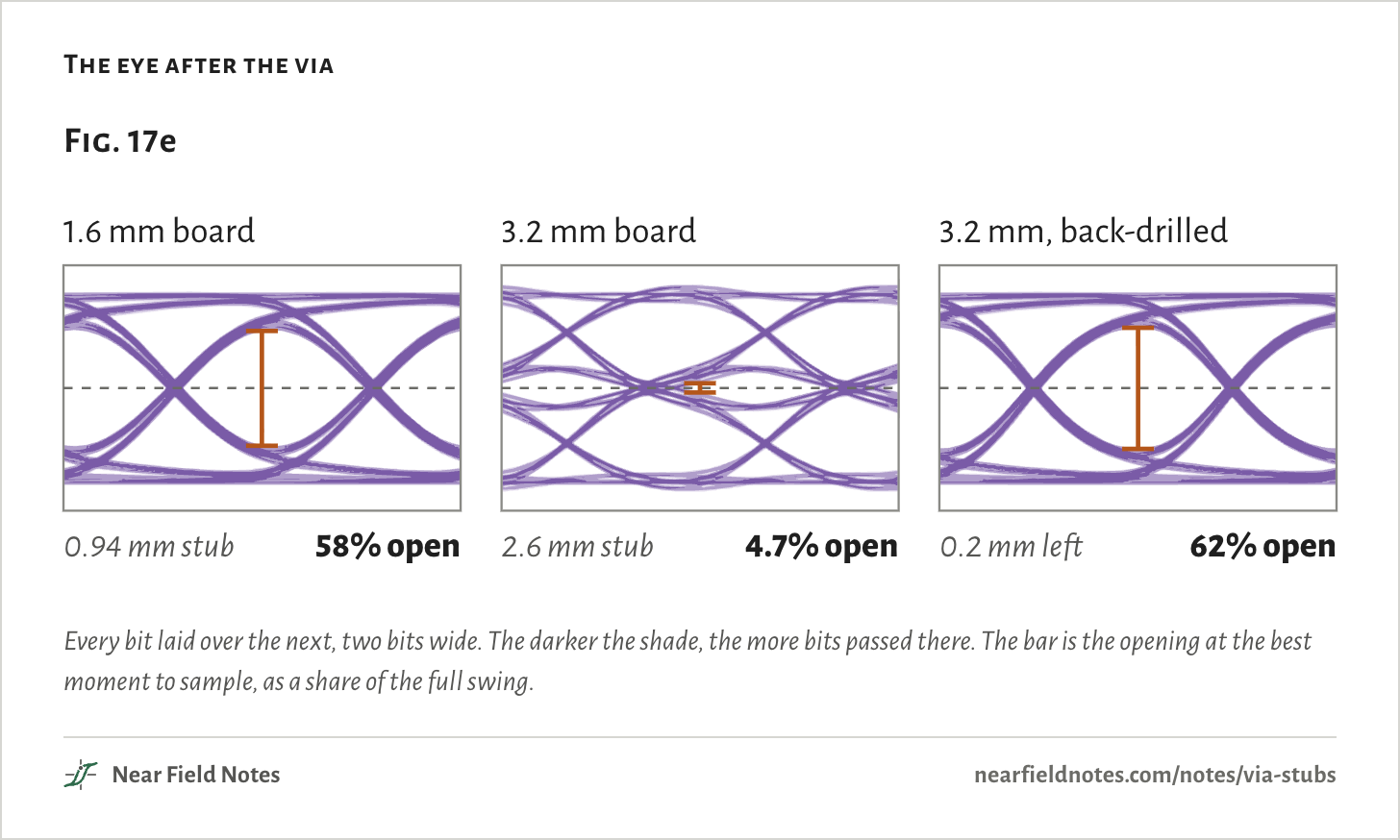
The decibels show up as closed eyes. These are 25 Gb/s of random bits after 5 cm of FR-4 and the via, with no equalization. Note 8 shows how an eye is built.

The eye after the via
Fig. 17e1.6 mm board0.94 mm stub58% open3.2 mm board2.6 mm stub4.7% open3.2 mm, back-drilled0.2 mm left62% openFig. 17e1.6 mm board0.94 mm stub58% open3.2 mm board2.6 mm stub4.7% open3.2 mm, back-drilled0.2 mm left62% openFig. 17e1.6 mm board0.94 mm stub58% open3.2 mm board2.6 mm stub4.7% open3.2 mm, back-drilled0.2 mm left62% open
Every bit laid over the next, two bits wide. The darker the shade, the more bits passed there. The bar is the opening at the best moment to sample, as a share of the full swing.
The numbers
Eye open at1.6 mm board3.2 mm board3.2 mm, back-drilled
Stub0.94 mm stub2.6 mm stub0.2 mm left
10 Gb/s79%78%79%
16 Gb/s71%61%72%
25 Gb/s58%4.7%62%
342

What each fix buys

The same via, four ways

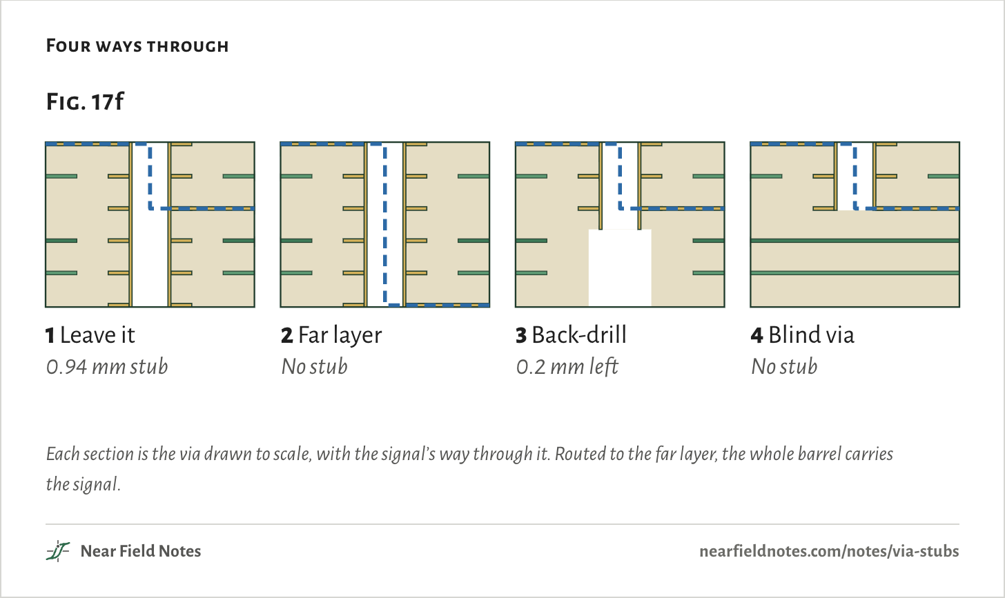
There are four ways to deal with a stub, cheapest first. Leaving it costs nothing. Routing the pair to the far layer costs nothing either, if the layer is free. Back-drilling adds a drilling step from the far side. A blind via needs a board built in stages, which is worth it only if the board needs that anyway.

Four ways through
Fig. 17f1 Leave it0.94 mm stub2 Far layerNo stub3 Back-drill0.2 mm left4 Blind viaNo stubFig. 17f1 Leave it0.94 mm stub2 Far layerNo stub3 Back-drill0.2 mm left4 Blind viaNo stubFig. 17f1 Leave it0.94 mm stub2 Far layerNo stub3 Back-drill0.2 mm left4 Blind viaNo stub
Each section is the via drawn to scale, with the signal’s way through it. Routed to the far layer, the whole barrel carries the signal.
The numbers
FixStubNotch
1Leave it0.94 mm stub37.4 GHz
2Far layerNo stubNone
3Back-drill0.2 mm left177 GHz
4Blind viaNo stubNone
344

Key to via stubs

Does this via need a fix?

  1. 1aStub shorter than 23.6 mm ÷ the lane’s GBdLeave it
  2. 1bStub longer than thatGo to 2
  3. 2aThe pair can leave on the far layerRoute it there
  4. 2bIt has to leave on an inner layerGo to 3
  5. 3aThe board is built in stages anywayA blind via
  6. 3bA standard boardBack-drill, 0.2 mm left

This board’s 0.94 mm stub passes 1a up to 25 GBd.

345

Conditions

Board
MNT Reform motherboard 3.0, 6 layers, 1.58 mm. Its design files are open hardware under CERN-OHL-S v2.
Stack-up
Six 35 µm copper layers and five 0.274 mm FR-4 layers, εr 4.5. The top trace sees 3.4 with the air above it.
Via
0.4 mm drill, 0.8 mm pads on every layer, planes cleared 0.3 mm around the pads. Top layer to layer 3: 0.62 mm of barrel used, 0.94 mm left below.
Where
The PCIe pairs from the processor module’s socket, U1, to the M.2 slot, J10
Model
Every piece is a transmission line: 12 mm of 50 Ω top trace in, the used barrel as a 45 Ω line, the stub as an open 45 Ω line, 12 mm of 50 Ω layer-3 trace out. Each pad on a layer the signal doesn’t use adds 0.05 pF to ground. Both ends matched. No loss in the via.
Solved
In time, by finite differences, for the pulse. In frequency, with chained ABCD matrices, for S21, the limits and the eyes. The two agree within 0.1 dB up to 34 GHz.
Pulse
1 V, 20 ps wide at half height
Eyes
NRZ, 1500 random bits, edges 0.35 of a bit long, 5 cm of FR-4 with a loss tangent of 0.02 before the via, no equalization
Links
Each standard’s published rate per lane, in GBd
Thicker boards
The layers below layer 3 spread out evenly. Everything above stays as built.

Simulated only. Nothing on this page has been measured on a board yet.

Limits

  • A line model, not a 3D field solve. The barrel’s 45 Ω and the pads’ 0.05 pF are set by hand, not solved, so the notch could sit a few GHz away.
  • One line on its own. The pair’s other line, the ground vias beside it and the space between the planes are left out. The RX vias have no ground via within 1.6 mm.
  • With no loss, the notches go all the way down. Real ones are shallower and a little wider.
  • The eyes are this via’s alone. A real link adds its connector, its package and its equalizer.

Files

  • viasim/line1d.pyThe pulse in time
  • viasim/freq.pyS21, the notch, the limits and the eyes
  • layout/site_board.pyWhere the pairs run, read from the board file

Sources

Like this note?

Rev 1 ·
  1. Rev 1First published

Each fix gets a line here, with the reader's name if they want credit.

Did it answer your question?

Want more on this?

Report a problem

What should the next note be? Ask for one