Near Field Notes

Note 10PowerRev 1Watch the video · 2:09

Zero-voltage switching

What is zero-voltage switching, and what does it save?

Turning a switch on only after a current has already pulled the voltage across it to zero. A pair of 80 V FETs switching 10 A at 48 V then loses 0.45 µJ per turn-on, instead of 2.6 µJ.

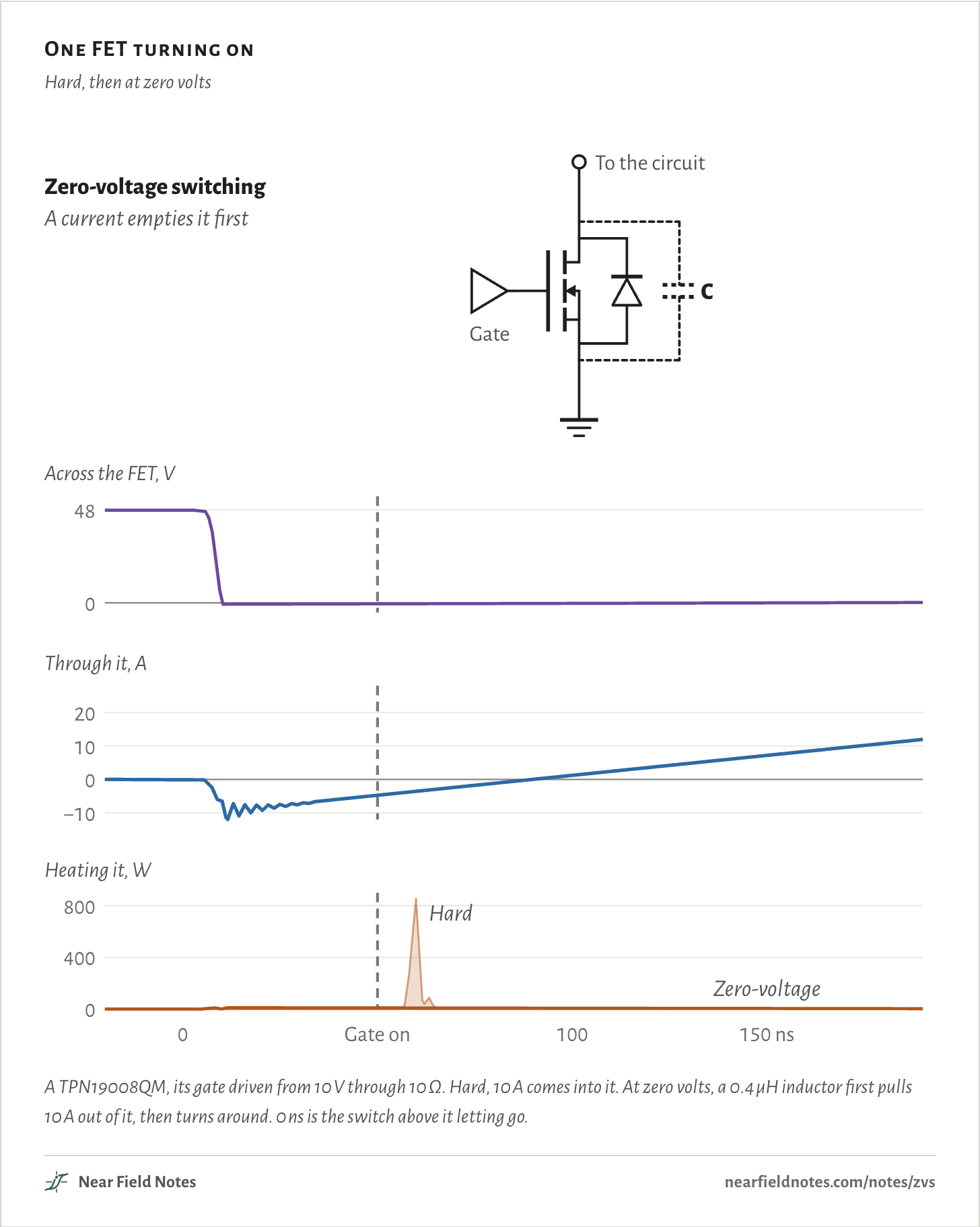
The figure turns one FET on twice. Hard, it takes on the current while 48 V is still across it, and for a few nanoseconds it heats at up to 860 W.

At zero volts, a current drains that voltage away before the gate comes on. By the time the FET conducts, there is almost nothing across it to turn into heat.

One FET turning on

Hard, then at zero volts

GateCTo the circuitHard switchingCurrent comes in at 48 VZero-voltage switchingA current empties it firstAcross the FET, V048Through it, A−1001020Heating it, W04008000Gate on100150 nsHardZero-voltageGateCTo the circuitHard switchingCurrent comes in at 48 VZero-voltage switchingA current empties it firstAcross the FET, V048Through it, A−1001020Heating it, W04008000Gate on100150 nsHardZero-voltageGateCTo the circuitHard switchingCurrent comes in at 48 VZero-voltage switchingA current empties it firstAcross the FET, V048Through it, A−1001020Heating it, W04008000Gate on100150 nsHardZero-voltage

A TPN19008QM, its gate driven from 10 V through 10 Ω. Hard, 10 A comes into it. At zero volts, a 0.4 µH inductor first pulls 10 A out of it, then turns around. 0 ns is the switch above it letting go.

Where the FET sits

The cell inside most converters

The FET never works alone. Most power converters pair it with a second switch and pass an inductor’s current back and forth between the two.

Only one switch is on at a time. Between turns comes a short dead time, here 50 ns, when both are off and the inductor’s current has to find its own way.

Each switch also has capacitance across it, drawn as C. At 48 V the pair holds Q=33.5 nC, and turning a switch on means moving that charge.

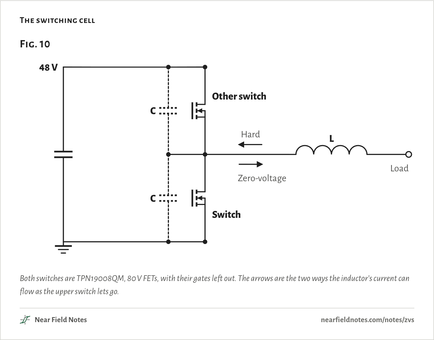
The way the inductor’s current flows as the upper switch lets go decides how the lower one turns on. Flowing into the node, the current holds it at 48 V, so the lower switch turns on hard.

Flowing out of the node, the current drains the lower switch’s C and fills the upper one’s. The voltage falls to zero by itself, before the gate comes on.

The switching cell
Fig. 1048 VOther switchSwitchCCLLoadHardZero-voltageFig. 1048 VOther switchSwitchCCLLoadHardZero-voltageFig. 1048 VOther switchSwitchCCLLoadHardZero-voltage

Both switches are TPN19008QM, 80 V FETs, with their gates left out. The arrows are the two ways the inductor’s current can flow as the upper switch lets go.

A capacitance that changes with voltage

Both switches, from the fitted model

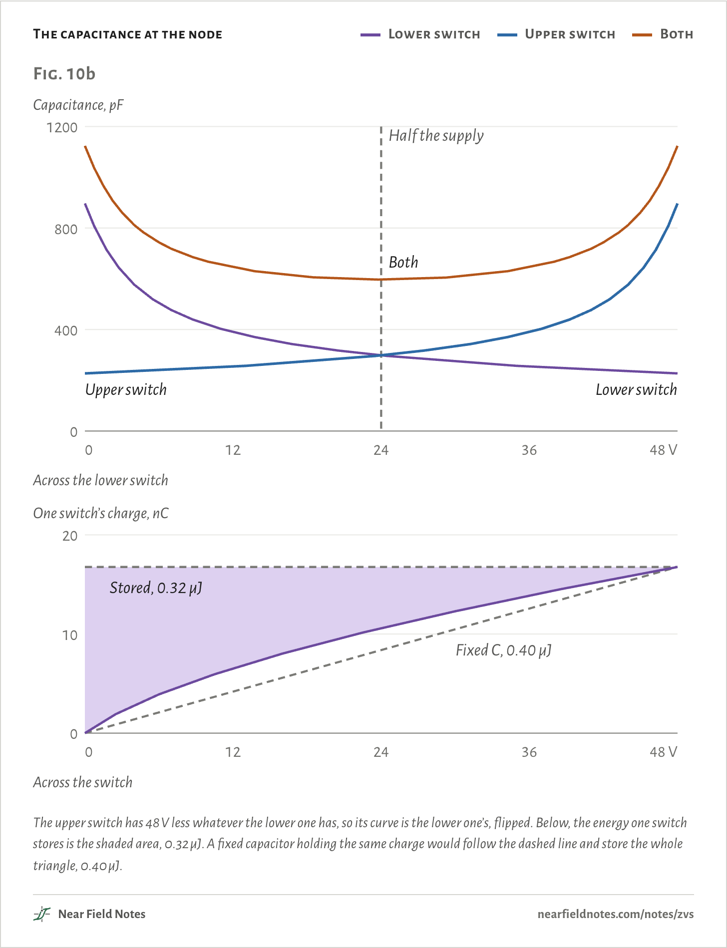
The C in Fig. 10 isn’t one number. A FET’s capacitance is largest near zero volts and falls as the voltage across it rises, in this one from 783 pF at 1 V to 227 pF at 48 V.

That’s why this page counts charge instead. Q adds the capacitance up over every volt the switch swings through, for both switches:

Q=2∫48 V0CdV

=2×16.7 nC=33.5 nC

The capacitance at the node
  • Lower switch
  • Upper switch
  • Both
Fig. 10bCapacitance, pF04008001200012243648 VAcross the lower switchHalf the supplyLower switchUpper switchBothOne switch’s charge, nC01020012243648 VAcross the switchStored, 0.32 µJFixed C, 0.40 µJFig. 10bCapacitance, pF04008001200012243648 VAcross the lower switchHalf the supplyLower switchUpper switchBothOne switch’s charge, nC01020012243648 VAcross the switchStored, 0.32 µJFixed C, 0.40 µJFig. 10bCapacitance, pF04008001200012243648 VAcross the lower switchHalf the supplyLower switchUpper switchBothOne switch’s charge, nC01020012243648 VAcross the switchStored, 0.32 µJFixed C, 0.40 µJ

The upper switch has 48 V less whatever the lower one has, so its curve is the lower one’s, flipped. Below, the energy one switch stores is the shaded area, 0.32 µJ. A fixed capacitor holding the same charge would follow the dashed line and store the whole triangle, 0.40 µJ.

240

Where a hard turn-on loses energy

10 A into the node, and out of it

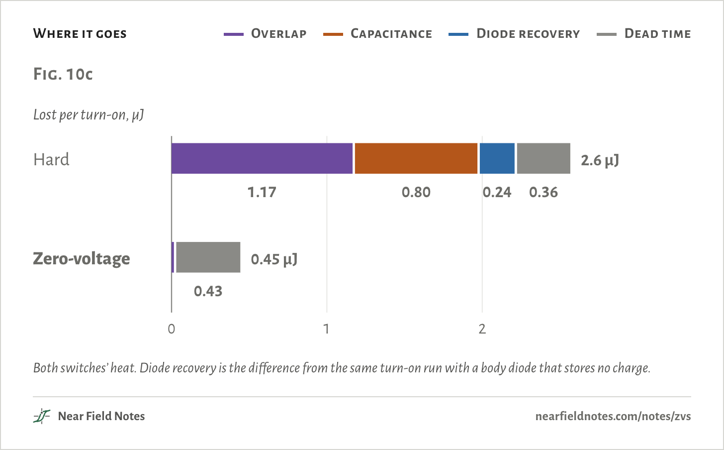
Start with the hard turn-on, the one most converters make every cycle. Its 2.6 µJ comes from four places, and turning on at zero volts removes three of them.

Where it goes
  • Overlap
  • Capacitance
  • Diode recovery
  • Dead time
Fig. 10cLost per turn-on, µJ012Hard1.170.800.240.362.6 µJZero-voltage0.430.45 µJFig. 10cLost per turn-on, µJ012Hard1.170.800.240.362.6 µJZero-voltage0.430.45 µJFig. 10cLost per turn-on, µJ012Hard1.170.800.240.362.6 µJZero-voltage0.430.45 µJ

Both switches’ heat. Diode recovery is the difference from the same turn-on run with a body diode that stores no charge.

242

Why a faster gate can’t fix it

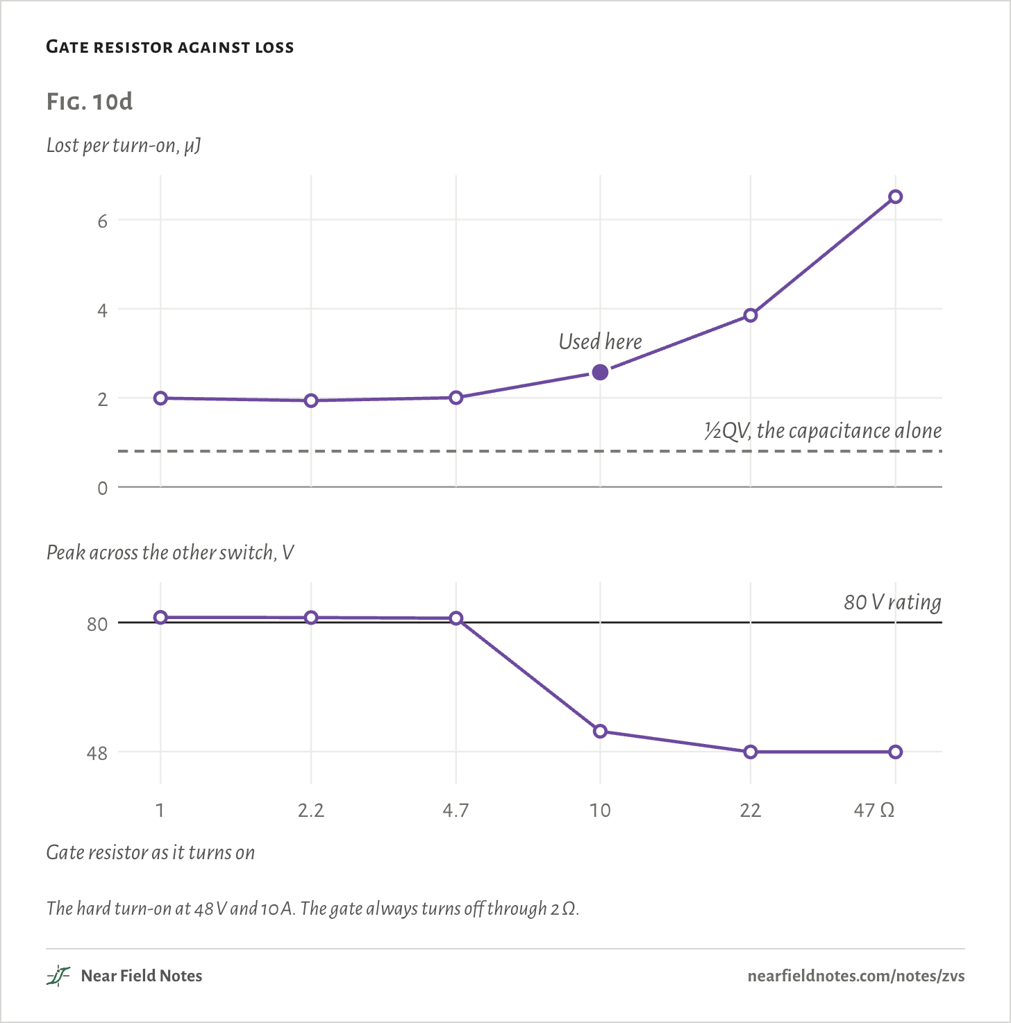
The hard turn-on at six gate resistors

The usual fix for switching loss is a faster gate. Driving it through less resistance shortens the overlap, so the loss falls from 6.5 µJ at 47 Ω to 2.0 µJ at 1 Ω.

Then it stops falling. A faster gate can’t shrink the capacitance’s ½QV or the dead time, and the diode’s recovery grows. The faster edge also makes the other switch ring to 81 V, past its 80 V rating.

Getting under that floor takes a different idea: get rid of the voltage before the switch turns on.

Gate resistor against loss
Fig. 10dLost per turn-on, µJPeak across the other switch, V0246488080 V rating12.24.7102247 ΩGate resistor as it turns on½QV, the capacitance aloneUsed hereFig. 10dLost per turn-on, µJPeak across the other switch, V0246488080 V rating12.24.7102247 ΩGate resistor as it turns on½QV, the capacitance aloneUsed hereFig. 10dLost per turn-on, µJPeak across the other switch, V0246488080 V rating12.24.7102247 ΩGate resistor as it turns on½QV, the capacitance aloneUsed here

The hard turn-on at 48 V and 10 A. The gate always turns off through 2 Ω.

How a current empties the switch

1 A out of the node, 50 ns of dead time

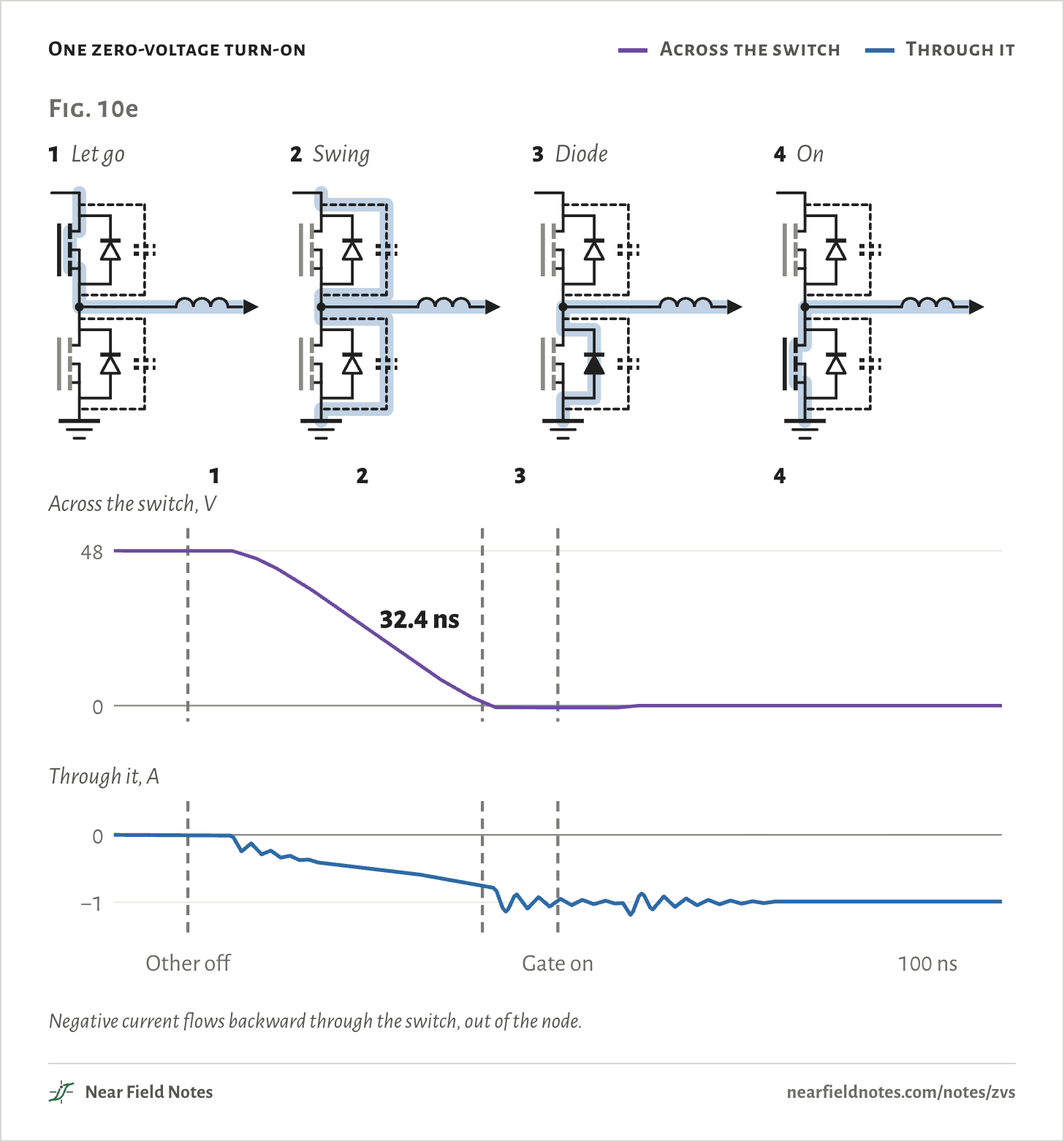
Run the inductor’s current out of the node and it does that for the switch. Here is the turn-on with just 1 A, slow enough to watch.

  1. Let go. The other switch turns off.
  2. Swing. The current pulls the charge out of the switch and into the other one, at a steady rate.
  3. Diode. At zero the switch’s own body diode catches the current.
  4. On. The gate comes on with nothing across the switch.

The swing moves Q at the rate the current flows, so the time it takes is

t=QI

=33.5 nC1 A=33.5 ns

Simulated, the swing takes 32.4 ns. Its energy goes back into the current instead of into heat.

Q already adds the capacitance up over every volt, so the rule holds whatever the curve’s shape.

The opening’s current was 10 A, so its swing took only 4.0 ns.

One zero-voltage turn-on
  • Across the switch
  • Through it
Fig. 10e1Let go2Swing3Diode4OnAcross the switch, V048Through it, A−10Other offGate on100 ns123432.4 nsFig. 10e1Let go2Swing3Diode4OnAcross the switch, V048Through it, A−10Other offGate on100 ns123432.4 nsFig. 10e1Let go2Swing3Diode4OnAcross the switch, V048Through it, A−10Other offGate on100 ns123432.4 ns

Negative current flows backward through the switch, out of the node.

How much current it takes

Every current against three dead times

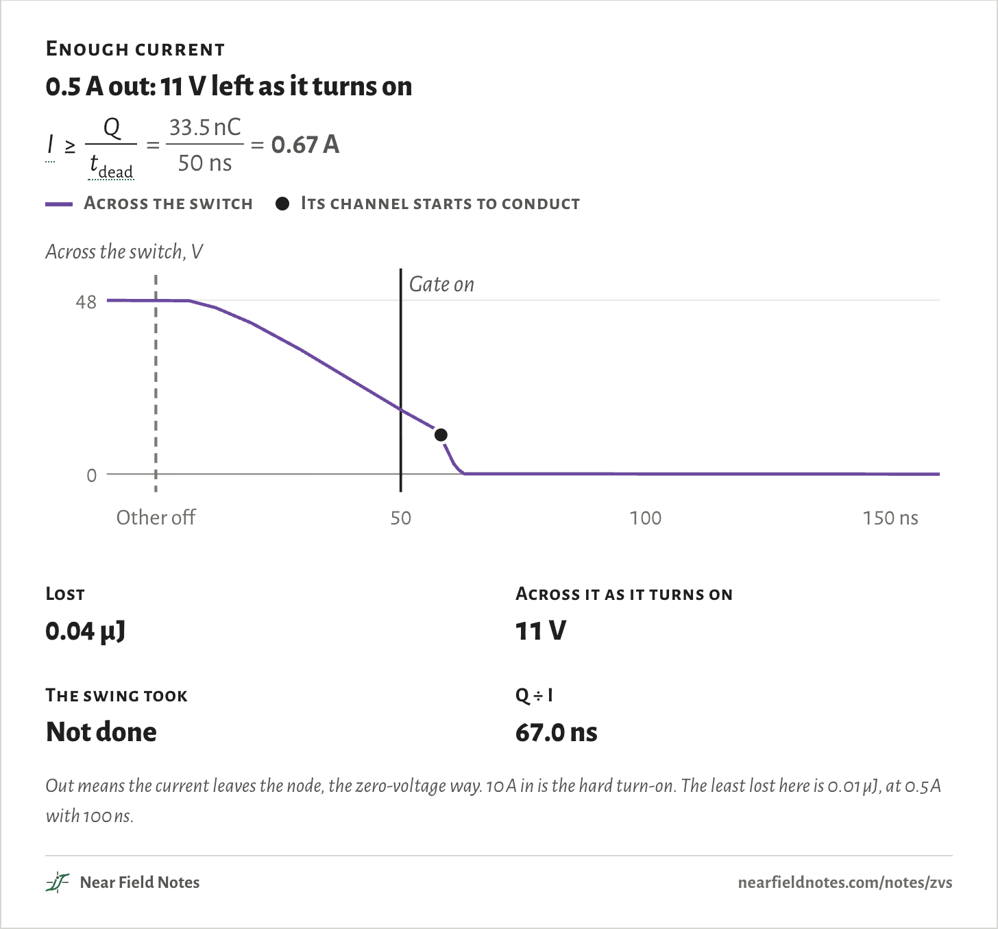
The swing has to finish inside the dead time, or the switch turns on with voltage still across it. That sets the least current that will do.

Too little leaves voltage for the turn-on to burn. Too much only keeps the diode conducting longer, which is why 10 A loses more than 1 A.

0.5 A out
Dead time
Enough current

0.5 A out: 11 V left as it turns on

I≥Qtdead=33.5 nC50 ns=0.67 A
  • Across the switch
  • Its channel starts to conduct
Across the switch, V048Other off50100150 nsGate onGate onGate onGate onGate onGate onGate onGate onGate onGate onGate onGate onGate onGate onGate onGate onGate onGate onGate onGate onGate onGate onGate onGate onAcross the switch, V048Other off50100150 nsGate onGate onGate onGate onGate onGate onGate onGate onGate onGate onGate onGate onGate onGate onGate onGate onGate onGate onGate onGate onGate onGate onGate onGate onAcross the switch, V048Other off50100150 nsGate onGate onGate onGate onGate onGate onGate onGate onGate onGate onGate onGate onGate onGate onGate onGate onGate onGate onGate onGate onGate onGate onGate onGate on
Lost
0.04 µJ
Across it as it turns on
11 V
The swing took
Not done
Q ÷ I
67.0 ns

Out means the current leaves the node, the zero-voltage way. 10 A in is the hard turn-on. The least lost here is 0.01 µJ, at 0.5 A with 100 ns.

When an inductor makes the current

1 µH, the switch held off

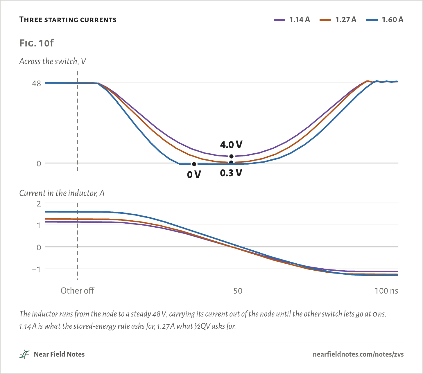
So far the current held steady through the swing, as it does in a large inductor. A small inductor’s current falls as the voltage swings against it.

The swing then runs on the energy the inductor stores, and the rule becomes one of energy instead of time. The energy to cover is ½QV, 0.80 µJ, more than the 0.65 µJ the capacitances store.

Three starting currents
  • 1.14 A
  • 1.27 A
  • 1.60 A
Fig. 10fAcross the switch, V048Current in the inductor, A−1012Other off50100 ns4.0 V0.3 VFig. 10fAcross the switch, V048Current in the inductor, A−1012Other off50100 ns4.0 V0.3 V0 VFig. 10fAcross the switch, V048Current in the inductor, A−1012Other off50100 ns4.0 V0.3 V0 V

The inductor runs from the node to a steady 48 V, carrying its current out of the node until the other switch lets go at 0 ns. 1.14 A is what the stored-energy rule asks for, 1.27 A what ½QV asks for.

244

What it saves

One turn-on every cycle

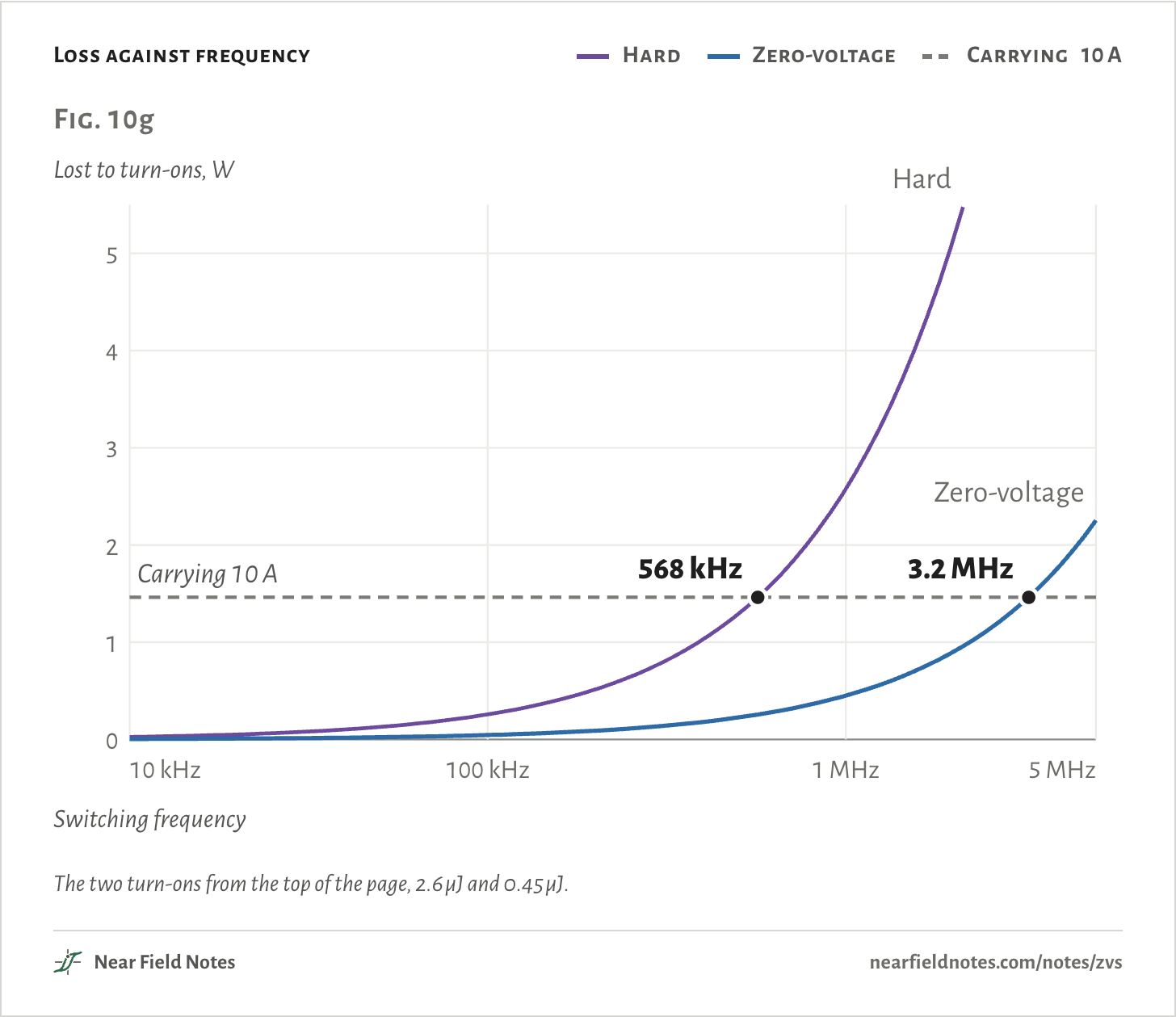
A converter pays its turn-on loss every cycle, so the loss grows with switching frequency: P=Ef.

At low frequency the two turn-ons cost little either way. Above a few hundred kilohertz the hard one costs more than carrying the current.

Loss against frequency
  • Hard
  • Zero-voltage
  • Carrying 10 A
Fig. 10gLost to turn-ons, W01234510 kHz100 kHz1 MHz5 MHzSwitching frequencyCarrying 10 AFig. 10gLost to turn-ons, W01234510 kHz100 kHz1 MHz5 MHzSwitching frequencyCarrying 10 A568 kHzHard3.2 MHzZero-voltageFig. 10gLost to turn-ons, W01234510 kHz100 kHz1 MHz5 MHzSwitching frequencyCarrying 10 A568 kHzHard3.2 MHzZero-voltage

The two turn-ons from the top of the page, 2.6 µJ and 0.45 µJ.

246

Zero-voltage circuits

Where the swinging current comes from

Every turn-on on this page used a current that was already there. A real converter has to arrange one, and the key sorts the usual ways.

Key to zero-voltage circuits

Where does the swinging current come from?

  1. 1aThe inductor’s current already flows out of the switch when the other lets goFree, like a buck’s low side
  2. 1bIt flows into the switchGo to 2
  3. 2aA small inductor can let its current reverse every cycleTriangular current mode
  4. 2bIt can’tGo to 3
  5. 3aA transformer is in the loopGo to 4
  6. 3bThere isn’t oneAn assist cell
  7. 4aIts magnetizing current is big enoughLLC, active-clamp flyback
  8. 4bIts leakage inductance has to supply itPhase-shifted full bridge

Each still has to meet one of the two rules on this page: enough current to move Q inside the dead time, or, from a small inductor, enough energy.

Conditions

Switches
Two Toshiba TPN19008QM, 80 V, with a model fitted by hand to the datasheet, as in Note 4. At 48 V each holds 16.7 nC.
Driver
An ideal 10 V source, on through 10 Ω, or 1 to 47 Ω in Fig. 10d, and off through 2 Ω, with 3 nH in each gate loop. 50 ns of dead time, 25 and 100 ns in the explorer.
Copper
1.3 nH from the 1 µF capacitor around the two switches
Current
10 A, held steady over the edge, into the node or out of it. In the opening’s zero-voltage pass, 0.4 µH to a steady 48 V instead, and 1 µH in Fig. 10f.
Heat
The opening shows the lower FET’s own. Everywhere else it is both switches’.
Lost
What both switches dissipate beyond carrying the current, from the other switch’s gate command until this one is on and settled 250 ns later. What their capacitance stores and gives back isn’t counted, and nor is the gate driver’s energy.
Solver
ngspice, at 27 °C

Simulated only. Nothing on this page has been measured on a board yet.

Limits

  • 81 V is the FET model’s breakdown. At gate resistors of 4.7 Ω and below the other switch’s ring reaches it, so its real peak would be higher.
  • The model’s capacitance and body diode are fitted to the datasheet’s curves, not measured.
  • A large inductor’s current changes a little over an edge. Here it is held steady.
  • The overlap is what’s left of the hard turn-on’s loss after the other three parts.

Files

  • zsim/general.pyThe switching cell, every run on this page and how the loss is counted
  • gatesim/fets.pyThe fitted FET model, from Note 4

Sources

Like this note?

Rev 1 ·
  1. Rev 1First published

Each fix gets a line here, with the reader's name if they want credit.

Did it answer your question?

Want more on this?

Report a problem

What should the next note be? Ask for one