Near Field Notes

Note 4PowerRev 1Watch the video · 0:12

Gate ringing

How hard should you drive a half bridge?

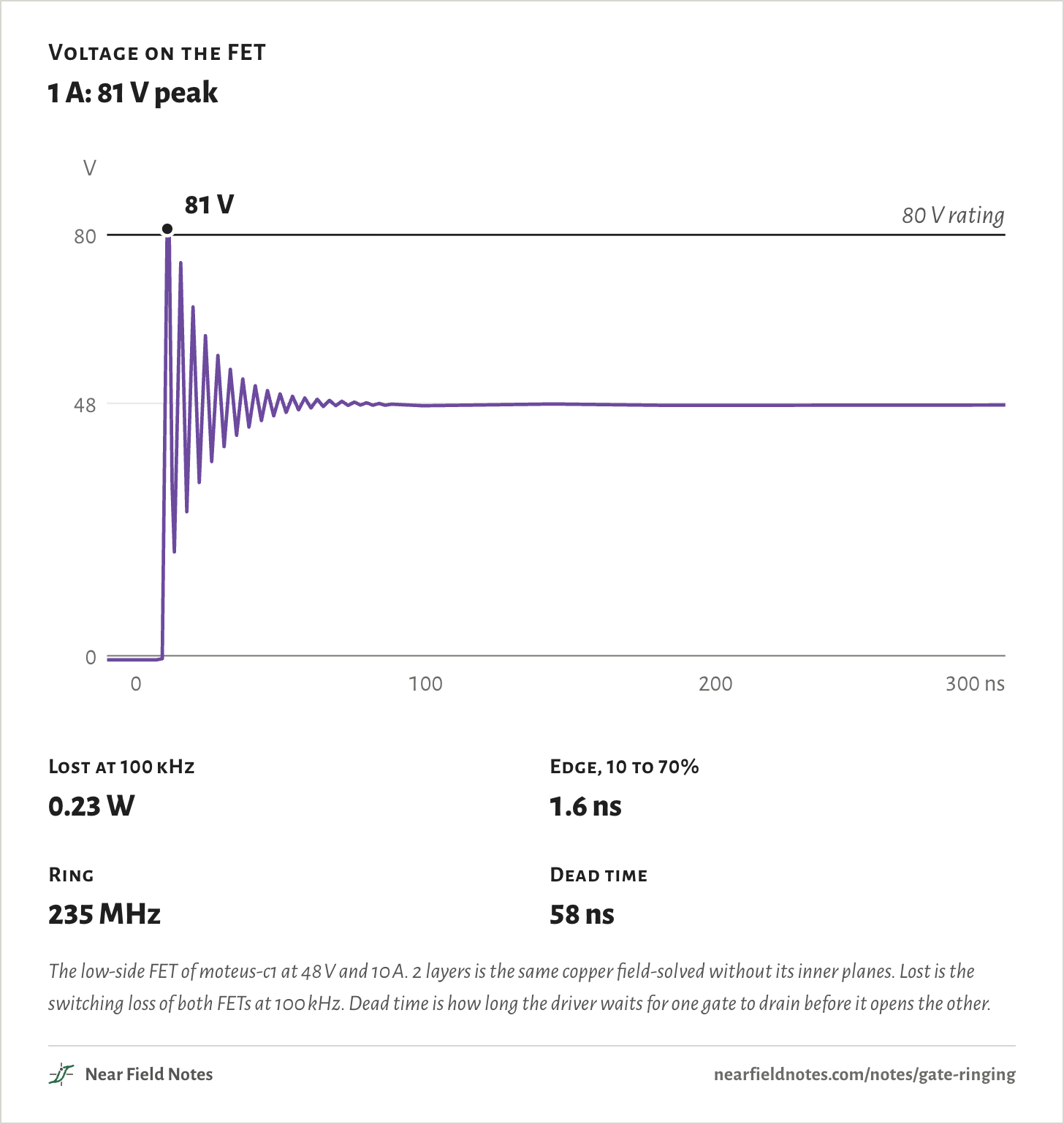
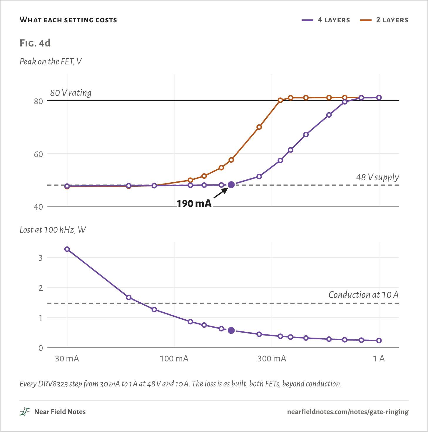
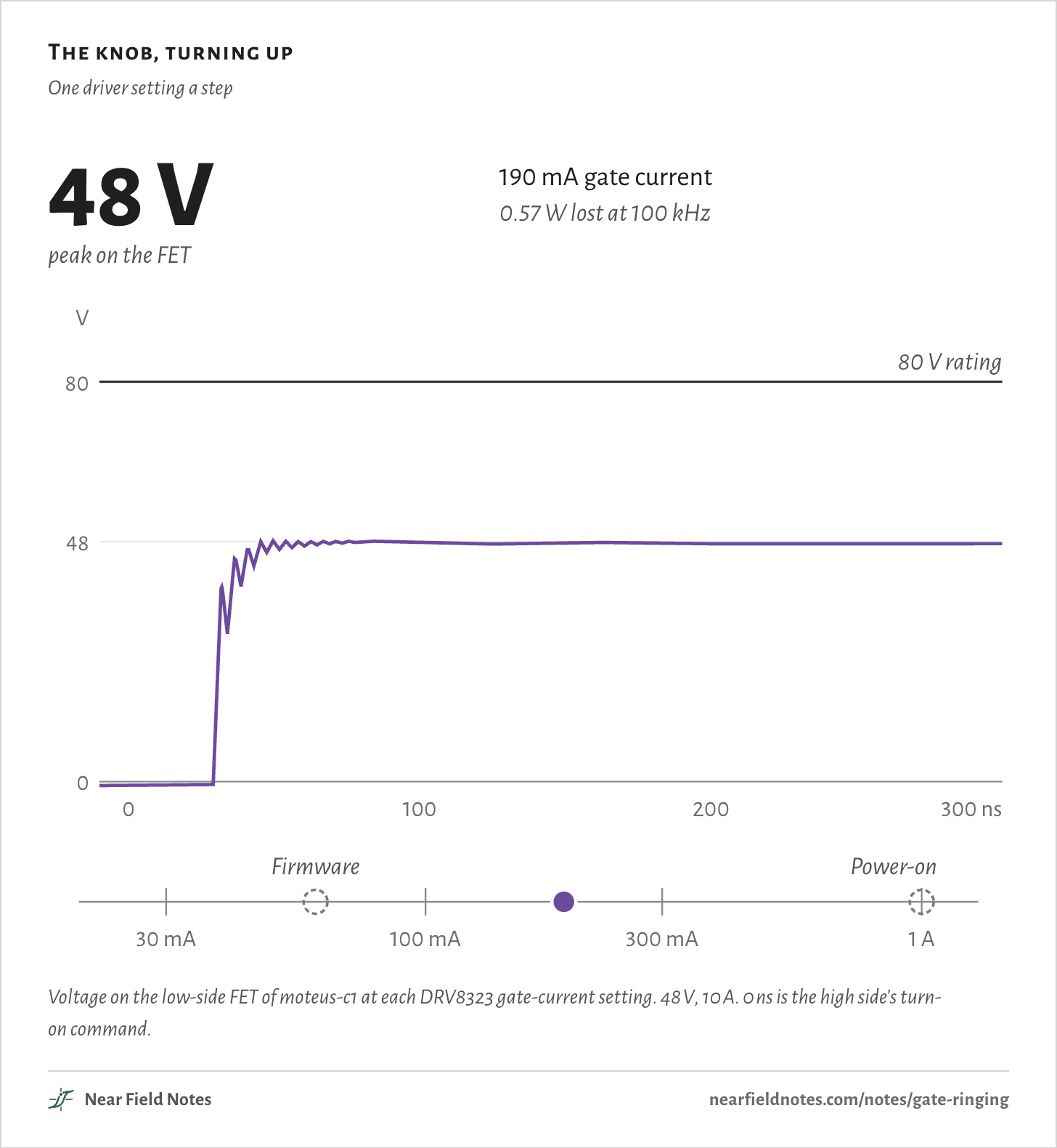
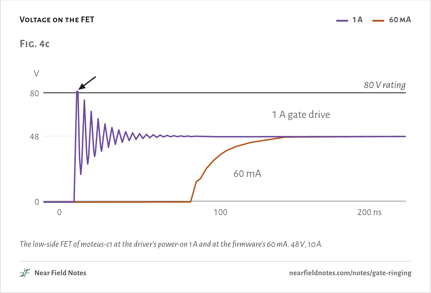
As hard as it goes without ringing. At its 1 A power-on setting, the gate driver on moteus-c1 rings its 80 V FET to 81 V at 48 V. 190 mA stays at 48 V, and 30 mA loses 3.3 W at 100 kHz.

The knob, turning up

One driver setting a step

48 V30 mA gate current3.3 W lost at 100 kHz48 V60 mA gate current1.7 W lost at 100 kHz48 V120 mA gate current0.86 W lost at 100 kHz48 V190 mA gate current0.57 W lost at 100 kHz51 V260 mA gate current0.44 W lost at 100 kHz57 V330 mA gate current0.37 W lost at 100 kHz67 V440 mA gate current0.31 W lost at 100 kHz80 V680 mA gate current0.26 W lost at 100 kHz81 V1 A gate current0.23 W lost at 100 kHzpeak on the FETV0488080 V rating0100200300 ns30 mA100 mA300 mA1 AFirmwarePower-on48 V30 mA gate current3.3 W lost at 100 kHz48 V60 mA gate current1.7 W lost at 100 kHz48 V120 mA gate current0.86 W lost at 100 kHz48 V190 mA gate current0.57 W lost at 100 kHz51 V260 mA gate current0.44 W lost at 100 kHz57 V330 mA gate current0.37 W lost at 100 kHz67 V440 mA gate current0.31 W lost at 100 kHz80 V680 mA gate current0.26 W lost at 100 kHz81 V1 A gate current0.23 W lost at 100 kHzpeak on the FETV0488080 V rating0100200300 ns30 mA100 mA300 mA1 AFirmwarePower-on48 V30 mA gate current3.3 W lost at 100 kHz48 V60 mA gate current1.7 W lost at 100 kHz48 V120 mA gate current0.86 W lost at 100 kHz48 V190 mA gate current0.57 W lost at 100 kHz51 V260 mA gate current0.44 W lost at 100 kHz57 V330 mA gate current0.37 W lost at 100 kHz67 V440 mA gate current0.31 W lost at 100 kHz80 V680 mA gate current0.26 W lost at 100 kHz81 V1 A gate current0.23 W lost at 100 kHzpeak on the FETV0488080 V rating0100200300 ns30 mA100 mA300 mA1 AFirmwarePower-on

Voltage on the low-side FET of moteus-c1 at each DRV8323 gate-current setting. 48 V, 10 A. 0 ns is the high side’s turn-on command.

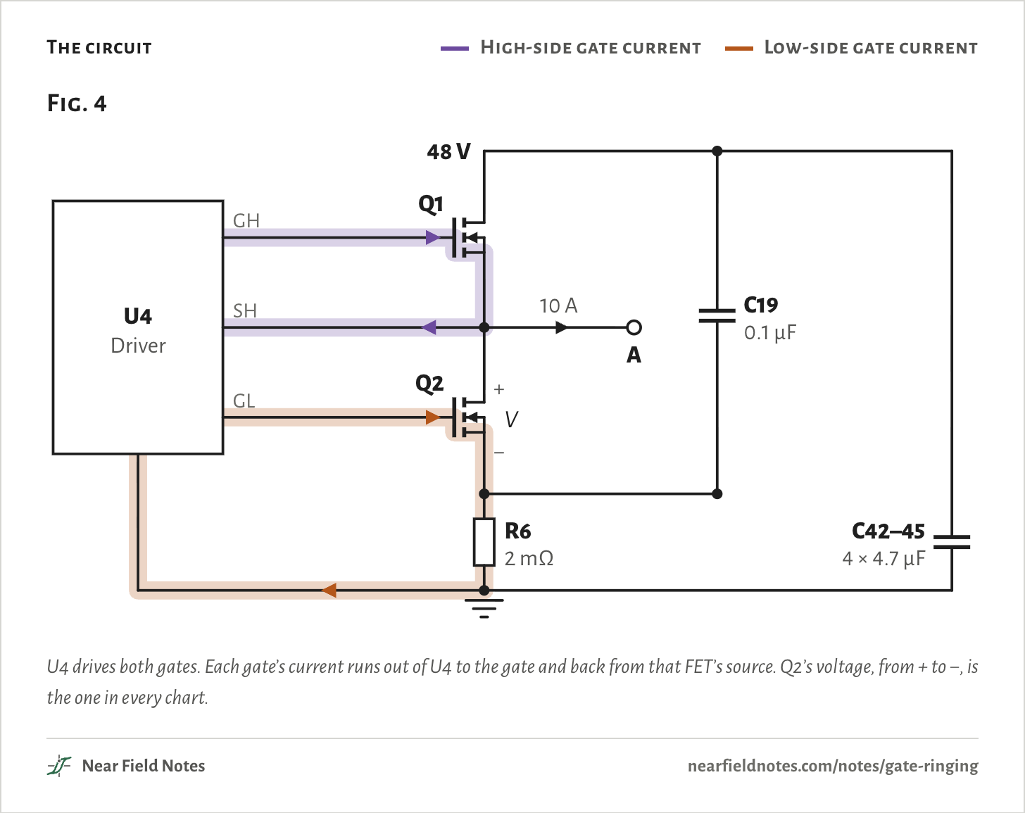
The gate drive loops

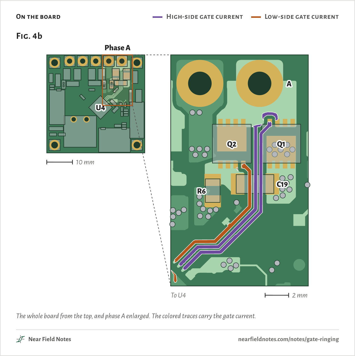
Phase A of moteus-c1 r1.2

One phase of mjbots’ moteus-c1 motor controller. The gate driver U4 turns the high-side FET Q1 on by pushing current into its gate. How hard it pushes, from 10 mA to 1 A, is the knob on this page. Every chart shows the voltage on the low-side FET Q2 as Q1 snaps on.

The circuit
  • High-side gate current
  • Low-side gate current
Fig. 448 VQ1Q2C190.1 µFR62 mΩC42–454 × 4.7 µF+−VA10 AU4DriverGHSHGLFig. 448 VQ1Q2C190.1 µFR62 mΩC42–454 × 4.7 µF+−VA10 AU4DriverGHSHGLFig. 448 VQ1Q2C190.1 µFR62 mΩC42–454 × 4.7 µF+−VA10 AU4DriverGHSHGL

U4 drives both gates. Each gate’s current runs out of U4 to the gate and back from that FET’s source. Q2’s voltage, from + to −, is the one in every chart.

On the board
  • High-side gate current
  • Low-side gate current
Fig. 4bU4Phase A10 mmQ1Q2C19R6ATo U42 mmFig. 4bU4Phase A10 mmQ1Q2C19R6ATo U42 mmFig. 4bU4Phase A10 mmQ1Q2C19R6ATo U42 mm

The whole board from the top, and phase A enlarged. The colored traces carry the gate current.

Voltage on the FET
  • 1 A
  • 60 mA
Fig. 4cV0488080 V rating0100200 ns1 A gate drive60 mAFig. 4cV0488080 V rating0100200 ns1 A gate drive60 mAFig. 4cV0488080 V rating0100200 ns1 A gate drive60 mA

The low-side FET of moteus-c1 at the driver’s power-on 1 A and at the firmware’s 60 mA. 48 V, 10 A.

48

Key to gate drive

How do you slow the edge?

  1. 1aThe driver sets its gate currentThe fastest step that doesn’t ring
  2. 1bThe driver has one strengthGo to 2
  3. 2aThe resistor that stops the ring lets the gate drain in timeThat gate resistor
  4. 2bIt drains so slowly that both FETs conductRg_on, with Rg_off and a diode across it

On moteus-c1 at 48 V the fastest step that doesn’t ring is 190 mA, and 120 mA without the inner planes. With a fixed 1.7 A driver, TI’s DRV8302, at 24 V, 33 Ω stops the ring. At 68 Ω both FETs conduct and lose 28 µJ a cycle. 68 Ω with 4.7 Ω and a diode across it loses 5 µJ. A slow gate changes which FET is best, as Note 20 shows.

Turn the knob yourself

Every driver setting, on 4 and 2 layers
Board
1 A
Voltage on the FET

1 A: 81 V peak

V0488080 V rating0100200300 ns51 V57 V61 V67 V75 V80 V81 V81 V51 V55 V58 V70 V80 V81 V81 V81 V81 V81 V81 VV0488080 V rating0100200300 ns51 V57 V61 V67 V75 V80 V81 V81 V51 V55 V58 V70 V80 V81 V81 V81 V81 V81 V81 VV0488080 V rating0100200300 ns51 V57 V61 V67 V75 V80 V81 V81 V51 V55 V58 V70 V80 V81 V81 V81 V81 V81 V81 V
Lost at 100 kHz
0.23 W
Edge, 10 to 70%
1.6 ns
Ring
235 MHz
Dead time
58 ns

The low-side FET of moteus-c1 at 48 V and 10 A. 2 layers is the same copper field-solved without its inner planes. Lost is the switching loss of both FETs at 100 kHz. Dead time is how long the driver waits for one gate to drain before it opens the other.

What each setting costs
  • 4 layers
  • 2 layers
Fig. 4dPeak on the FET, VLost at 100 kHz, W30 mA100 mA300 mA1 A40608080 V rating48 V supply0123Conduction at 10 A190 mAFig. 4dPeak on the FET, VLost at 100 kHz, W30 mA100 mA300 mA1 A40608080 V rating48 V supply0123Conduction at 10 A190 mAFig. 4dPeak on the FET, VLost at 100 kHz, W30 mA100 mA300 mA1 A40608080 V rating48 V supply0123Conduction at 10 A190 mA

Every DRV8323 step from 30 mA to 1 A at 48 V and 10 A. The loss is as built, both FETs, beyond conduction.

50

Conditions

Board
mjbots moteus-c1 r1.2, phase A
FETs
Toshiba TPN19008QM, 80 V, with a model fitted by hand to the datasheet
Driver
TI DRV8323S, modeled from its datasheet’s gate-current steps, with no gate resistors
Load
48 V, with 10 A leaving the switch node, so the high side switches hard
Copper
Loop and gate inductances from an openEMS solve of all four layers: a 1.83 nH loop as built, 4.03 nH with the inner planes taken out
Loss
The energy both FETs lose in a cycle beyond conduction, times 100 kHz
Solver
ngspice, 48 runs. The driver’s 10 mA step doesn’t finish its edge in the 700 ns on-time, so it isn’t shown.

Simulated only. Nothing on this page has been measured on a board yet.

Limits

  • 81 V is the FET model’s breakdown. From 680 mA up the peak reads 80 to 81 V because the model avalanches. Without that clamp the ring would go higher.
  • The loss in the FET’s capacitance is a guess, 0.3 Ω. At 1 A the peak reads 81 V up to 0.3 Ω, 78 V at 1 Ω and 58 V at 3 Ω.
  • A probe on the pins sees the off gate swing from −3.4 to +4.8 V at 1 A. The gate inside the package swings from −0.9 to +1.3 V. Part of what the probe reads is the package’s own inductance.

Files

  • gatesim/bench.pyThe half bridge, its driver and the board’s copper
  • gatesim/fets.pyThe FET model and its datasheet check
  • fieldsim/model.pyThe four copper layers, as the field solver saw them

Sources

Like this note?

Rev 1 ·
  1. Rev 1First published

Each fix gets a line here, with the reader's name if they want credit.

Did it answer your question?

Want more on this?

Report a problem

What should the next note be? Ask for one