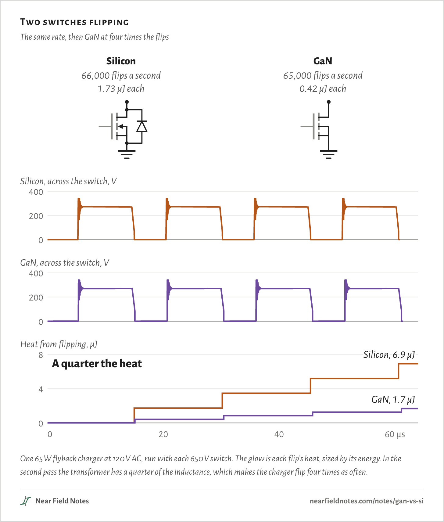
Because a GaN switch and its driver lose about a quarter as much energy each time it flips. In the same 65 W charger at 120 V AC, that’s 1.73 µJ a flip for silicon and 0.42 µJ for GaN, so GaN can flip four times as often for the same heat. A charger that flips faster needs a smaller transformer.
The figure runs both switches in one charger circuit. First they flip at the same rate, and silicon’s heat piles up four times as fast.
Then GaN flips 263,000 times a second. Its heat piles up at about silicon’s rate again.
Two switches flipping
The same rate, then GaN at four times the flips
One 65 W flyback charger at 120 V AC, run with each 650 V switch. The glow is each flip’s heat, sized by its energy. In the second pass the transformer has a quarter of the inductance, which makes the charger flip four times as often.
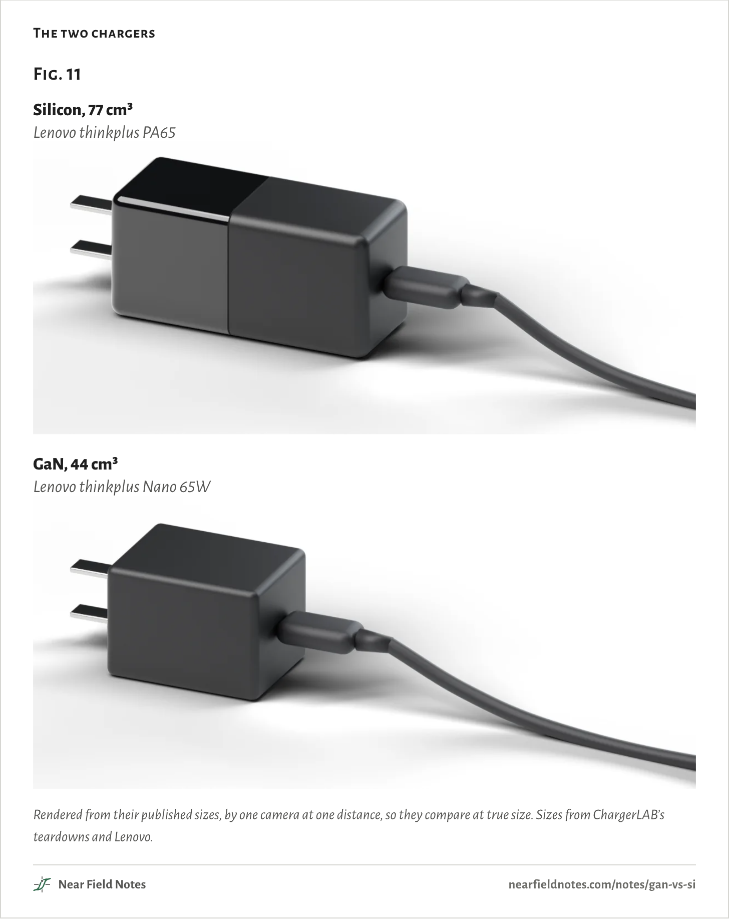
Two 65 W chargers
Lenovo’s silicon one and its GaN one
Lenovo sells two 65 W USB-C chargers with the same output. The thinkplus PA65 switches with an Infineon CoolMOS, a silicon FET. The thinkplus Nano switches with a Navitas GaN chip.
The GaN one is 44 cm³ against 77 cm³, 43% smaller.
Neither maker publishes its circuit, so this page simulates one charger of its own. It runs once with a 650 V silicon switch and once with a 650 V GaN switch of about the same resistance, and follows where the difference comes from.
The two chargers
Rendered from their published sizes, by one camera at one distance, so they compare at true size. Sizes from ChargerLAB’s teardowns and Lenovo.
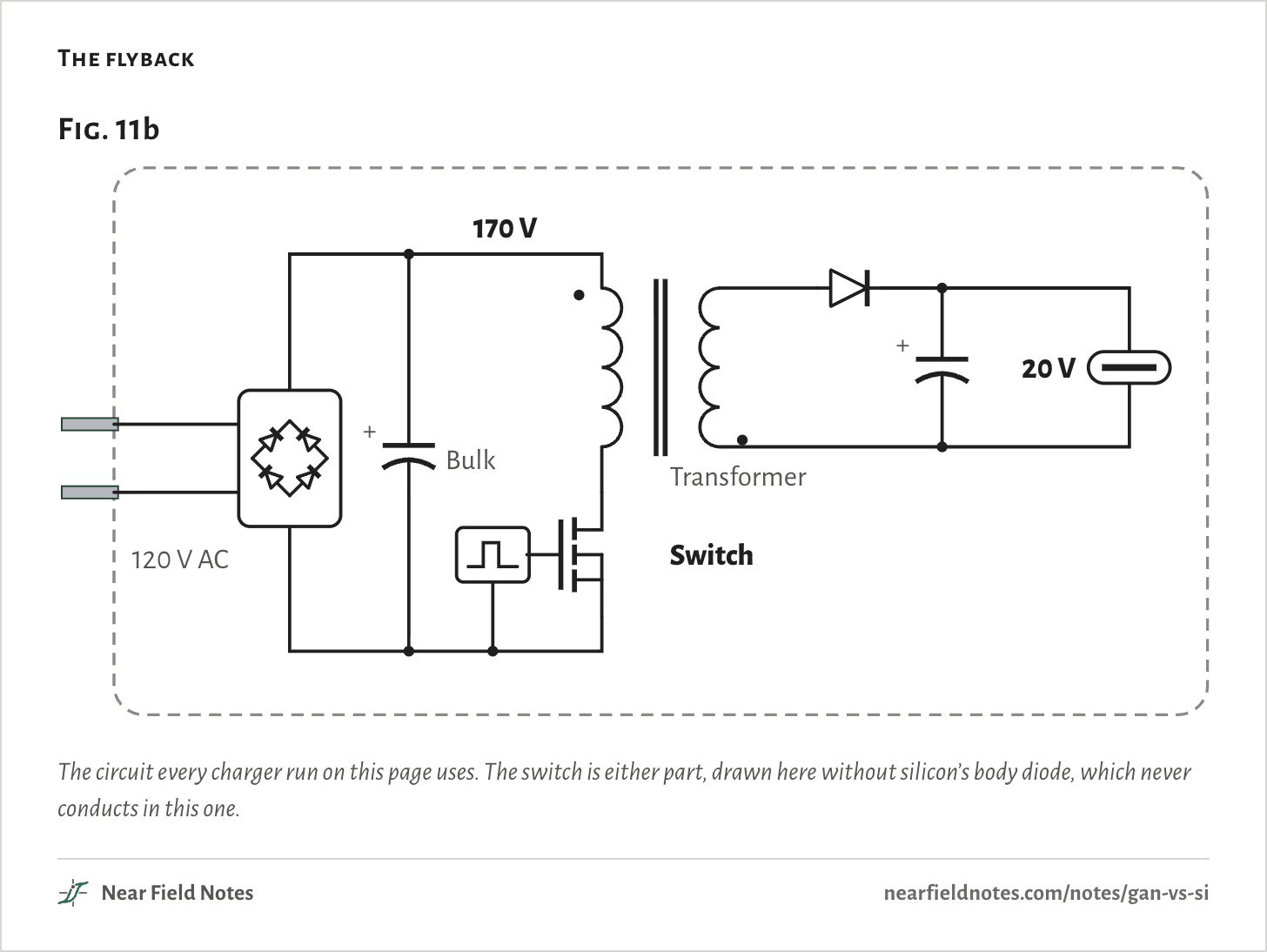
The circuit inside
A flyback, one switch
Most chargers this size are flybacks. The wall’s 120 V AC is rectified onto a bulk capacitor at about 170 V.
One switch connects the transformer’s first winding across those 170 V, filling its core with energy, then lets go. The energy comes out of the second winding into the USB-C port at 20 V.
Each on and off is one flip. With this transformer the charger flips about 66,000 times a second.
After letting go, the voltage across the switch rings down. This charger waits for the low point, the valley, before turning on again. That’s 72 V with silicon and 84 V with GaN.
The flyback
The circuit every charger run on this page uses. The switch is either part, drawn here without silicon’s body diode, which never conducts in this one.
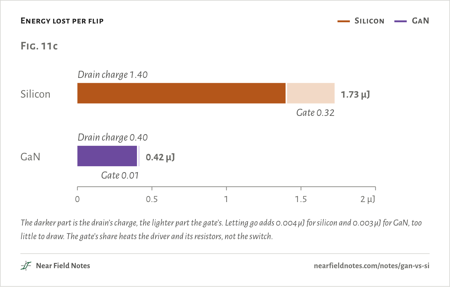
Where a flip’s energy goes
One flip at 120 V AC
A flip loses energy in three places. Turning on at the valley, the switch dumps the charge stored on its own drain through its channel. The gate driver fills the gate and empties it again. Letting go, the switch carries current for a moment while the voltage rises.
The drain’s charge is most of it for both switches: 1.40 µJ for silicon against 0.40 µJ for GaN. The gate adds 0.32 µJ to silicon’s and almost nothing to GaN’s.
At 66,000 flips a second, silicon’s 1.73 µJ a flip comes to 0.11 W of heat.
Energy lost per flip
Silicon
GaN
The darker part is the drain’s charge, the lighter part the gate’s. Letting go adds 0.004 µJ for silicon and 0.003 µJ for GaN, too little to draw. The gate’s share heats the driver and its resistors, not the switch.
The charge on the drain
Both switches, from the fitted models
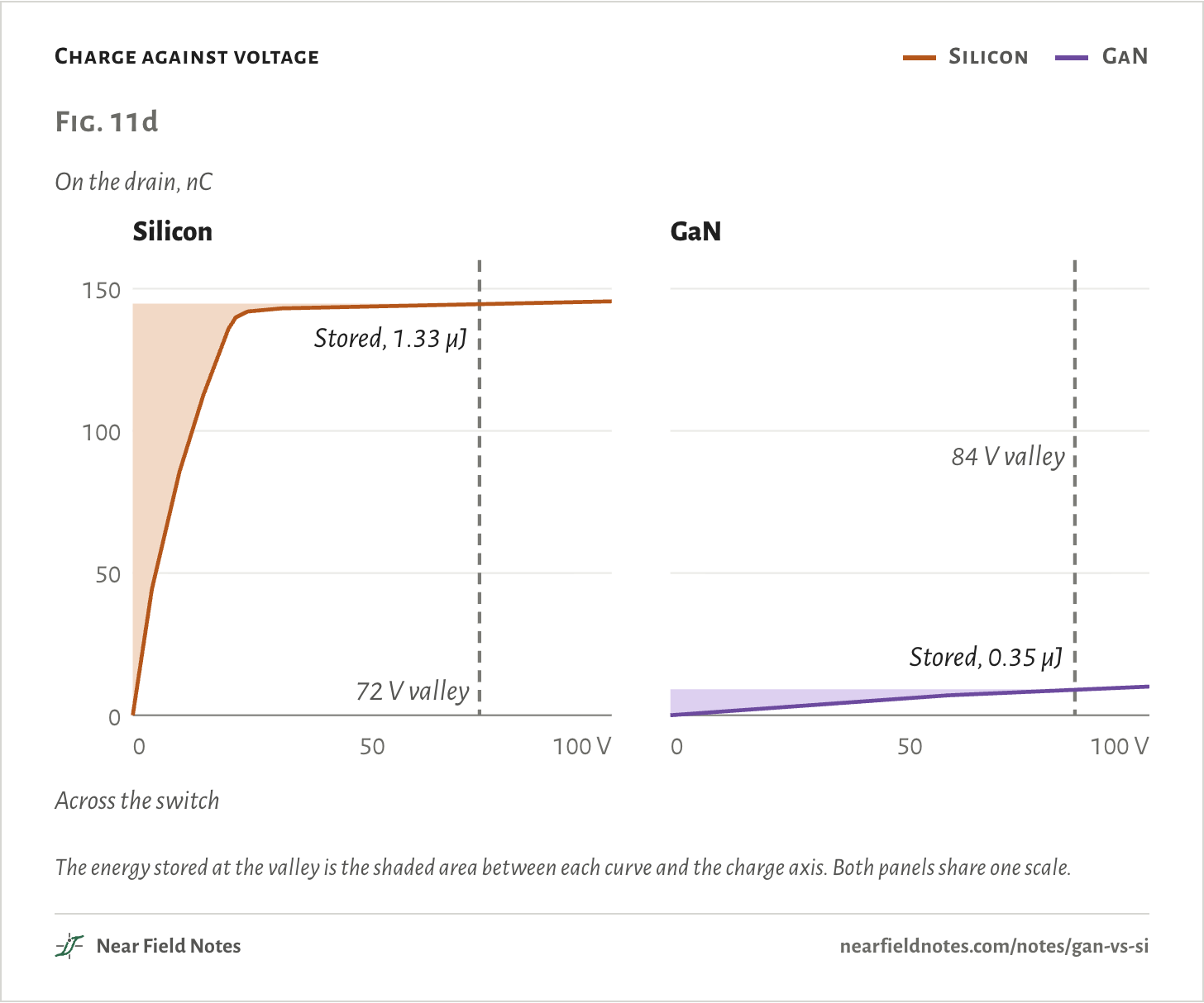
Every switch stores charge on its drain as the voltage across it rises. The energy that charge holds at the valley is what turning on throws away:
E=∫Qvalley0VdQ
=1.33 µJfor silicon,0.35 µJfor GaN
That’s most of what Fig. 11c counts for the drain. The rest is mostly the transformer winding’s own capacitance, emptied through the switch along with it.
Charge against voltage
Silicon
GaN
The energy stored at the valley is the shaded area between each curve and the charge axis. Both panels share one scale.
264
Output charge
Alike at 400 V, four times apart at the valley
Field marks. Datasheets give the energy on the drain at 400 V: 2.7 µJ for this silicon switch, 2.4 µJ for this GaN one.
Look-alike. By that number the two look alike. A flyback turns on near its valley, though, and silicon packs 94% of its charge below 25 V, so it’s nearly all there at the valley: 1.33 µJ against GaN’s 0.35 µJ.
Range. At 400 V silicon holds 151 nC, GaN 19 nC.
Habitat. Any switch that turns on with voltage across it pays this, hard or at a valley. Zero-voltage switching, Note 10, borrows it from a current instead.
265
Why GaN holds less
The stretch that holds 650 V
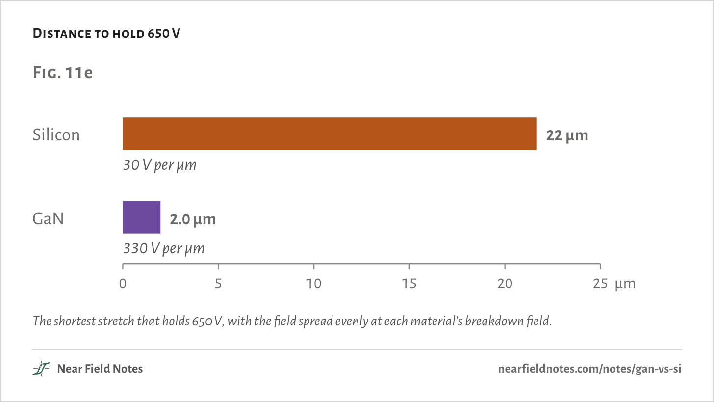
A switch holds its voltage across a stretch of material between drain and source. Each material breaks down past a certain field: about 30 V per µm in silicon, 330 V per µm in GaN.
So GaN holds 650 V in about a tenth of the distance, 2.0 µm against 22 µm. A shorter path conducts better, so a GaN chip reaches the same resistance at a fraction of the size.
A smaller chip has less area to store charge on its drain.
Distance to hold 650 V
The shortest stretch that holds 650 V, with the field spread evenly at each material’s breakdown field.
The gate
From each datasheet
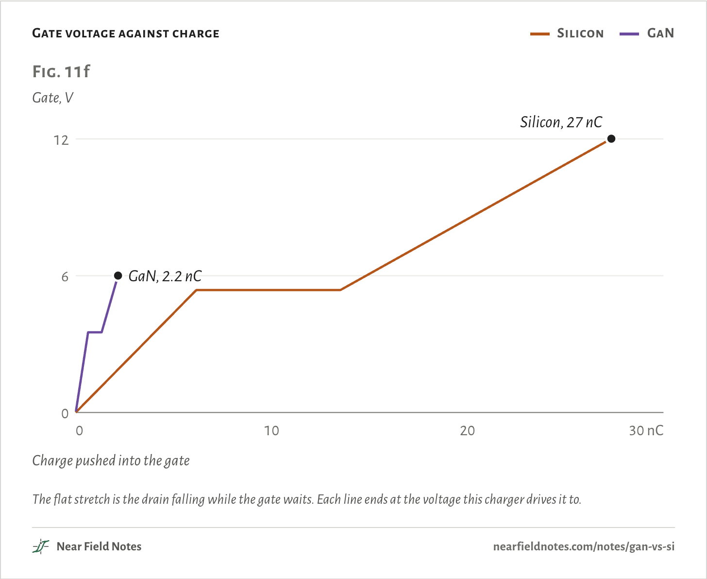
The smaller chip also has a smaller gate. Silicon’s takes about 27 nC to reach 12 V. GaN’s takes 2.2 nC to reach 6 V.
The driver spends E=QV every flip, about 0.32 µJ for silicon and 0.012 µJ for GaN.
Gate voltage against charge
Silicon
GaN
The flat stretch is the drain falling while the gate waits. Each line ends at the voltage this charger drives it to.
The edge
Both switches, the same 10 Ω driver
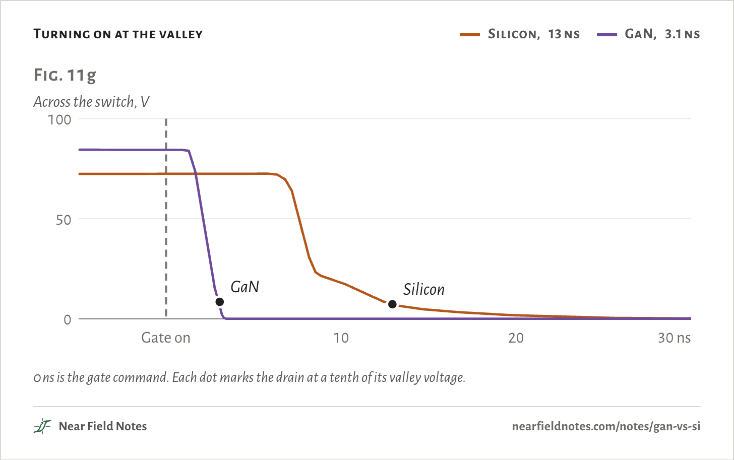
A small gate fills fast, so GaN switches faster from the same driver. Its drain falls in 3.1 ns, silicon’s in 13 ns.
In this charger the speed hardly matters. The switch turns on with no current flowing yet. It lets go into its own drain charge, which holds the voltage down while the current stops.
Speed and stored charge count for far more when two switches share a leg.
Turning on at the valley
Silicon, 13 ns
GaN, 3.1 ns
0 ns is the gate command. Each dot marks the drain at a tenth of its valley voltage.
Two switches on one leg
400 V, 5 A through the bottom switch
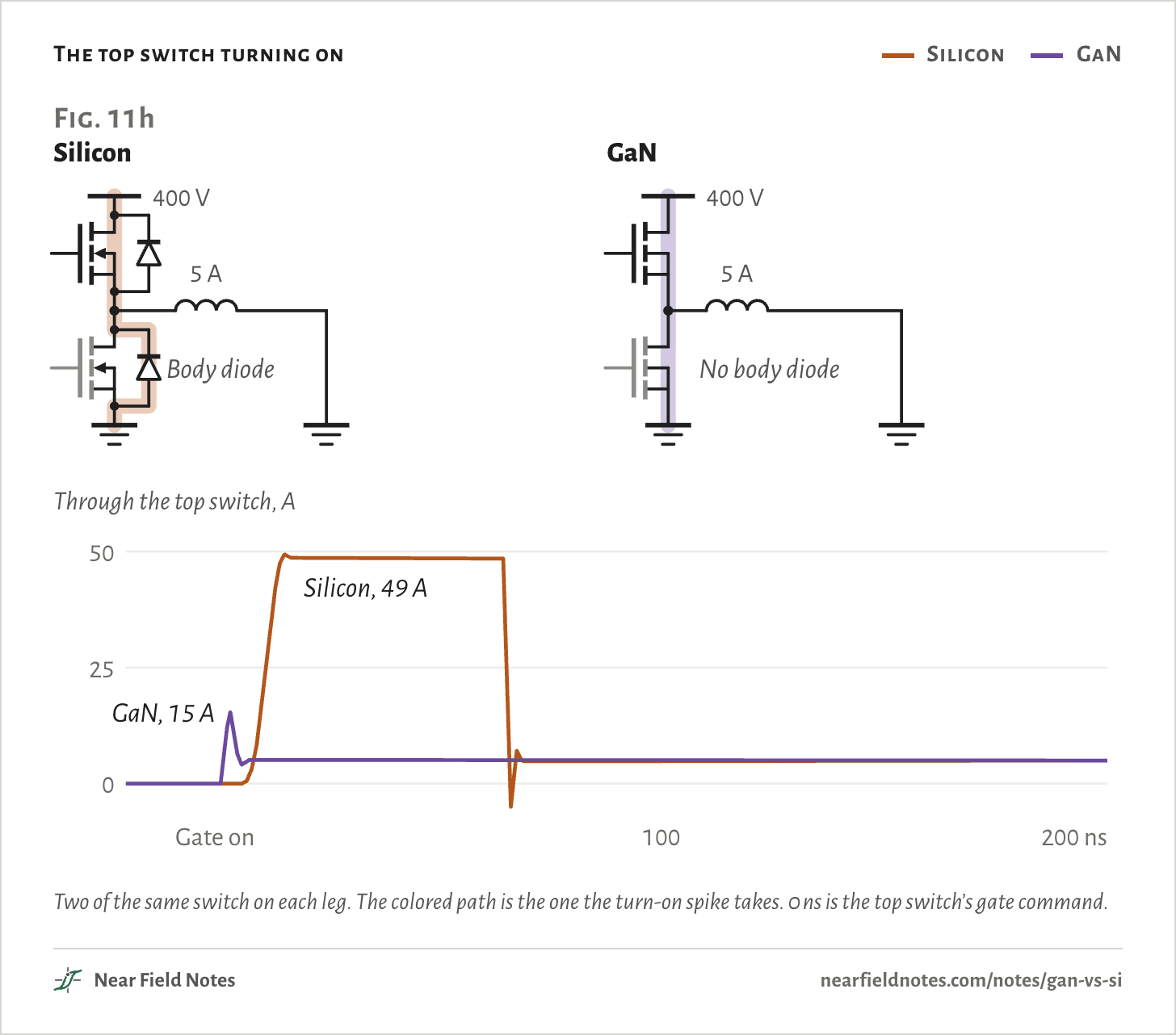
Bigger chargers, motor drives and power factor stages stack two switches on one leg. While the bottom one is off, the load’s current often runs backwards through it.
When the top switch turns on, it has to take that current over. With silicon, it first has to empty the bottom switch’s body diode.
The top switch turning on
Silicon
GaN
Two of the same switch on each leg. The colored path is the one the turn-on spike takes. 0 ns is the top switch’s gate command.
266
Reverse recovery
The charge a body diode stores
Field marks. Current running backwards through silicon’s body diode fills it with charge. The top switch has to pull it out at full voltage, 2,336 nC here.
Look-alike. GaN runs backwards through its own channel and stores nothing there. Its 20 nC is only the charge on its drain.
Range. The top switch’s current spikes to 49 A with silicon and 15 A with GaN. The turn-on costs 1,046 µJ against 18 µJ.
Habitat. Any leg where one switch hands its current to the other’s diode. The flyback above has one switch, so it never meets this.
267
What GaN gives up
From each datasheet, and the leg above
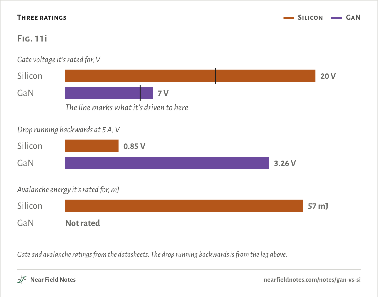
GaN’s gate is fragile. It’s rated −10 to +7 V, or up to +10 V for a microsecond or less. It’s driven to 6 V, so a few volts of ringing on the gate reach its limit. Silicon’s is rated ±20 V and driven to 12 V.
Running backwards, GaN’s channel drops 3.26 V at 5 A, where silicon’s body diode drops 0.85 V. Every nanosecond of dead time costs GaN about four times as much.
Silicon is rated to absorb 57 mJ if a spike drives it past its voltage. GaN has no avalanche rating. It’s rated for 850 V spikes and nothing above that.
Three ratings
Silicon
GaN
Gate and avalanche ratings from the datasheets. The drop running backwards is from the leg above.
Flipping faster
The charger at seven transformer sizes
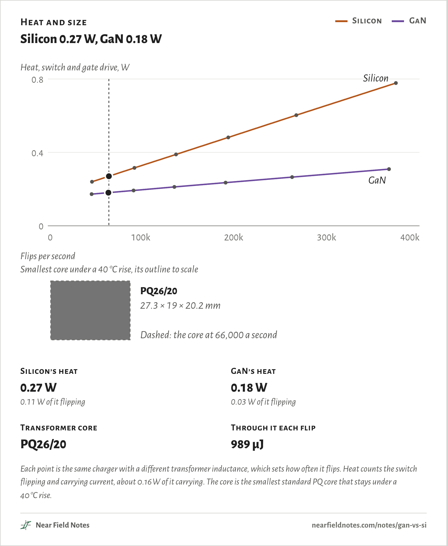
Back in the charger, the heat from flipping is the energy per flip times the flips per second, P=Ef. A quarter of the energy buys four times the flips.
Flipping faster shrinks the transformer. It has to pass the full 65 W, so each flip carries E=P/f: 989 µJ at 66,000 flips a second, 247 µJ at 263,000. Less energy a flip fits in a smaller core.
Heat and size
Silicon 0.27 W, GaN 0.18 W
Silicon
GaN
Silicon’s heat
0.27 W0.11 W of it flipping
GaN’s heat
0.18 W0.03 W of it flipping
Transformer core
PQ26/20
Through it each flip
989 µJ
Each point is the same charger with a different transformer inductance, which sets how often it flips. Heat counts the switch flipping and carrying current, about 0.16 W of it carrying. The core is the smallest standard PQ core that stays under a 40 °C rise.
At 263,000 flips a second, GaN heats as much as silicon does at 66,000: 0.265 W against 0.270 W.
Silicon can flip faster too. At 138,000 it already gets the smallest core here, for 0.39 W, 44% more heat than at 66,000. GaN gets the same core and runs cooler at every rate.
What GaN can’t shrink
The bulk capacitor at 120 V AC
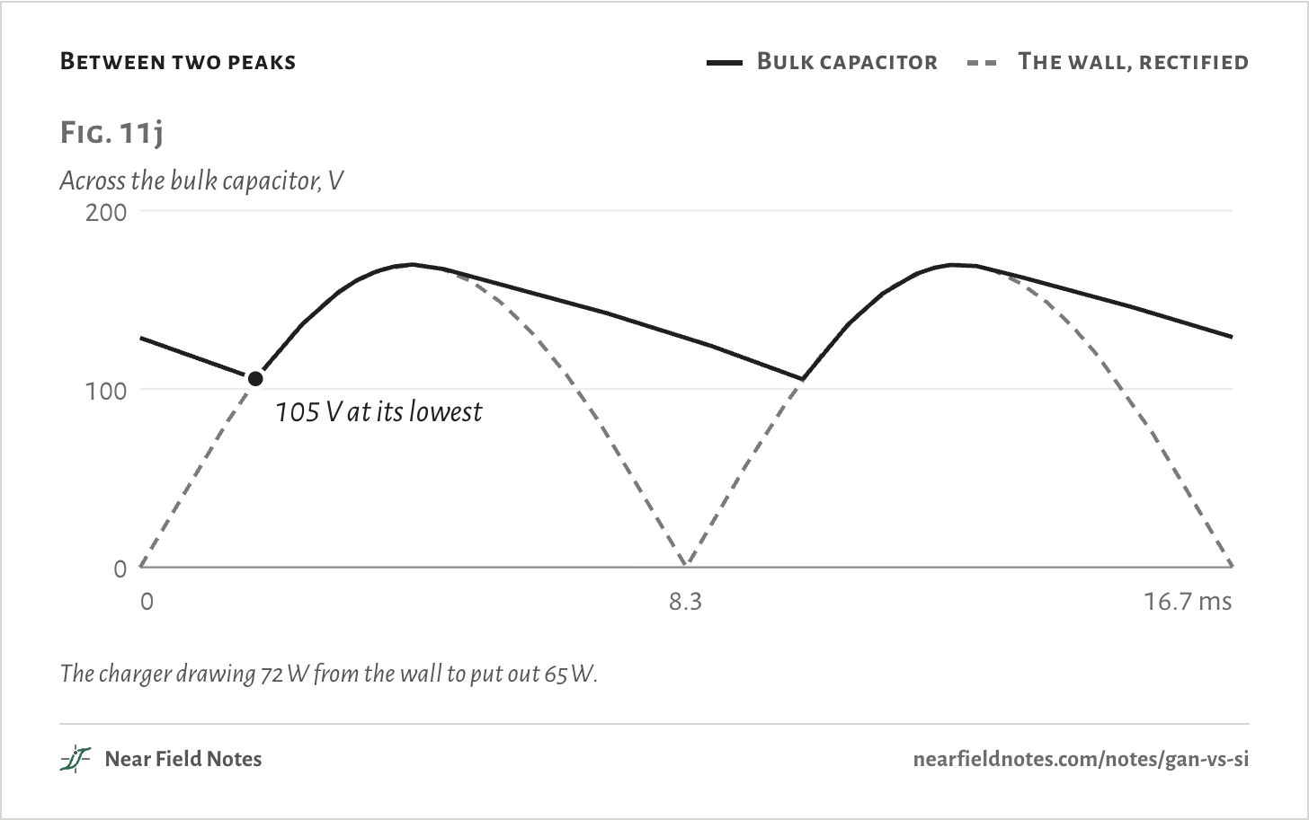
The bulk capacitor carries the charger between the wall’s peaks, 120 times a second. Its size is set by the wall’s 60 Hz, whatever the switch does.
Here 47 µF keeps the bus at 105 V or more. A 22 µF capacitor would let it sag to 31 V.
That takes a 400 V capacitor about 16 mm across and 25 mm long, whichever switch the charger uses.
Between two peaks
Bulk capacitor
The wall, rectified
The charger drawing 72 W from the wall to put out 65 W.
Conditions
Switches
Infineon IPD65R190C7, a 650 V CoolMOS C7, 168 mΩ. GaN Systems GS-065-011-1-L, a 650 V GaN transistor, 150 mΩ. Each with a model fitted to its datasheet. At 400 V they store 2.7 µJ and 2.4 µJ by their datasheets.
Charger
A quasi-resonant flyback from 120 V AC, a 170 V bus, a 5 to 1 transformer and 20 V at 3.25 A out. 430 µH of magnetizing inductance, 600 to 70 µH in the explorer and 100 µH in the opening’s second pass.
Driver
12 V for silicon and 6 V for GaN, on through 10 Ω and off through 3 Ω
Flip
One turn-on and one turn-off. Its energy counts the switch’s losses and the driver’s gate charge times its voltage.
Leg
Two of the same switch at 400 V, 5 A flowing backwards through the bottom one as the top one turns on
Cores
Ferroxcube PQ geometry in TDK PC95 ferrite, losses at 100 °C, rise from TDK’s measured figures for a wound PQ core
Solver
ngspice
Simulated only. Nothing on this page has been measured on a board yet.
Limits
The circuit is this page’s own, not either Lenovo charger’s. Their frequencies and cores aren’t published, and their switches are other parts: a CoolMOS P7 in the PA65 and a Navitas NV6134 in the Nano.
At 230 V AC the valley sits higher and the gap narrows: 2.55 µJ a flip for silicon, 1.66 µJ for GaN.
The models are fitted to datasheet curves, not measured.
The distance in Fig. 11e is the ideal for an evenly spread field. Superjunction silicon like the CoolMOS beats it with columns of alternating doping, which is also why its charge sits below 25 V.
Files
gsim/flyback.pyThe charger, every flip on this page and how its loss is counted
gsim/models.pyThe two switch models, fitted in gsim/fit.py