Near Field Notes

Note 7FabRev 1Watch the video · 0:14

Thermal relief

Should a ground pin tie into the plane through a thermal relief?

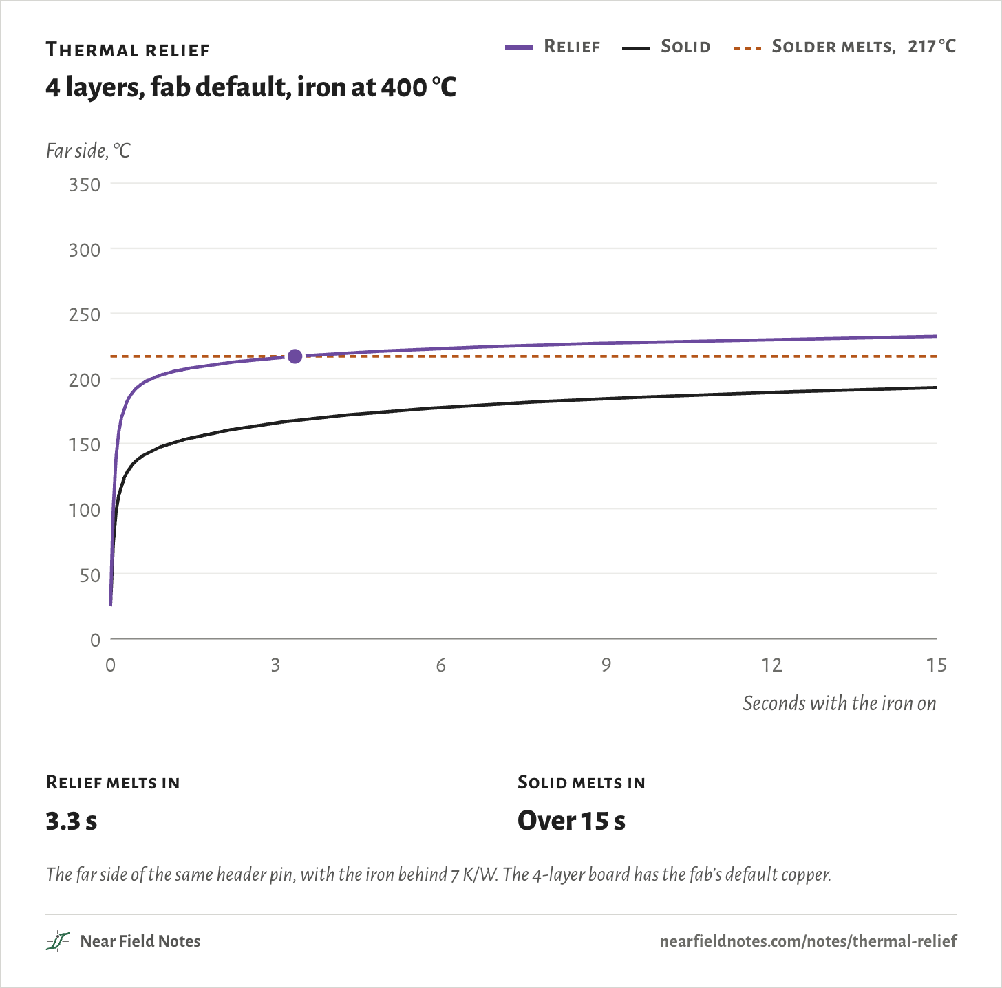
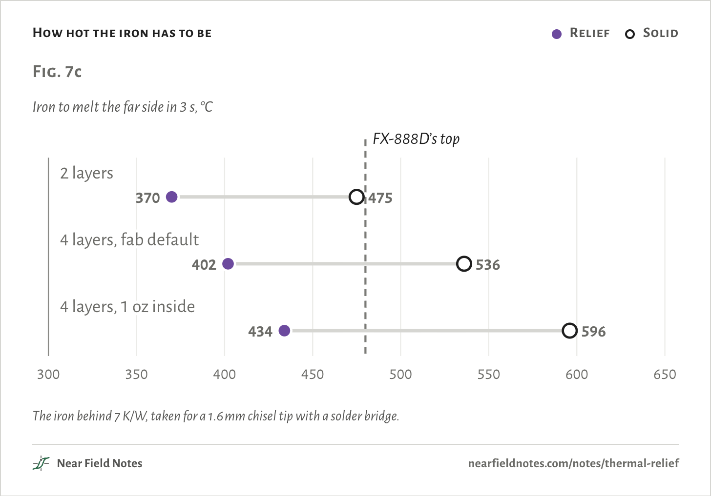
Yes, if it gets soldered. On a 4-layer board with the fab’s default copper, a 402 °C iron melts the solder on the far side through KiCad’s default spokes in 3 s. Tied in solid, it needs 536 °C. A Hakko FX-888D tops out at 480 °C.

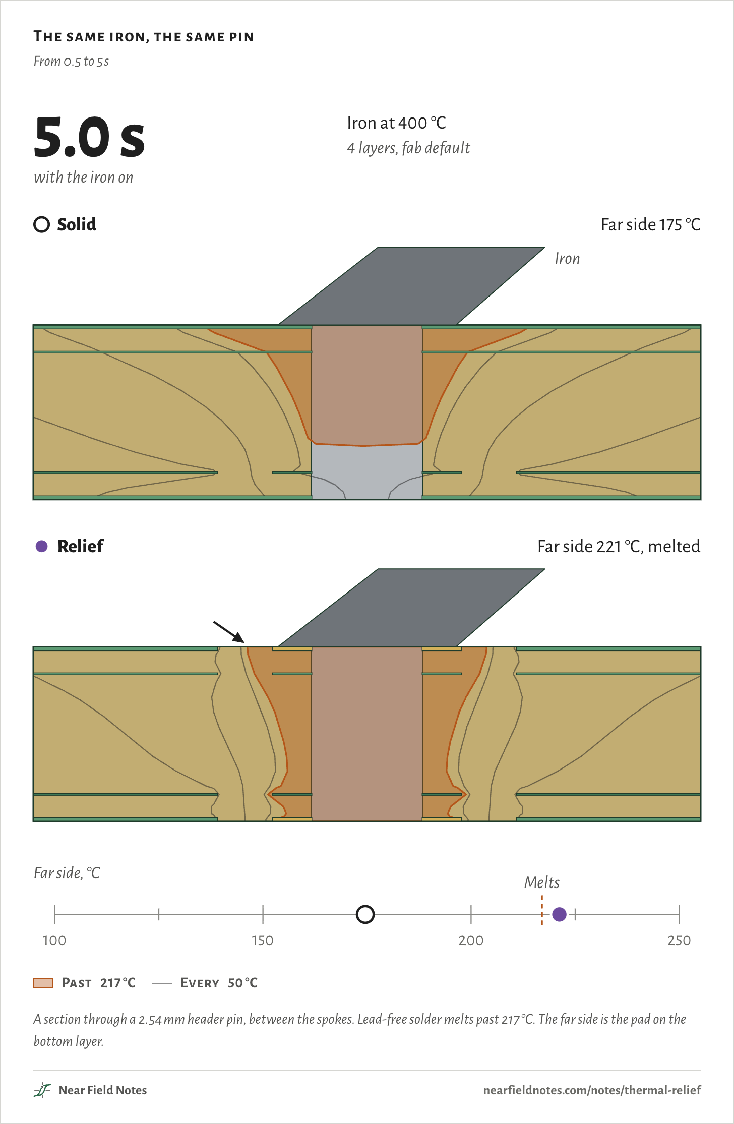
The same iron, the same pin

From 0.5 to 5 s

0.5 s1.0 s2.0 s3.0 s3.3 s5.0 swith the iron onIron at 400 °C4 layers, fab defaultSolidFar side 138 °CFar side 149 °CFar side 159 °CFar side 166 °CFar side 168 °CFar side 175 °CIronReliefFar side 194 °CFar side 204 °CFar side 212 °CFar side 216 °CFar side 217 °C, meltedFar side 221 °C, meltedFar side, °C100150200250Melts0.5 s1.0 s2.0 s3.0 s3.3 s5.0 swith the iron onIron at 400 °C4 layers, fab defaultSolidFar side 138 °CFar side 149 °CFar side 159 °CFar side 166 °CFar side 168 °CFar side 175 °CIronReliefFar side 194 °CFar side 204 °CFar side 212 °CFar side 216 °CFar side 217 °C, meltedFar side 221 °C, meltedFar side, °C100150200250Melts0.5 s1.0 s2.0 s3.0 s3.3 s5.0 swith the iron onIron at 400 °C4 layers, fab defaultSolidFar side 138 °CFar side 149 °CFar side 159 °CFar side 166 °CFar side 168 °CFar side 175 °CIronReliefFar side 194 °CFar side 204 °CFar side 212 °CFar side 216 °CFar side 217 °C, meltedFar side 221 °C, meltedFar side, °C100150200250Melts
  • Past 217 °C
  • Every 50 °C

A section through a 2.54 mm header pin, between the spokes. Lead-free solder melts past 217 °C. The far side is the pad on the bottom layer.

What a thermal relief is

KiCad’s default, on a header pin

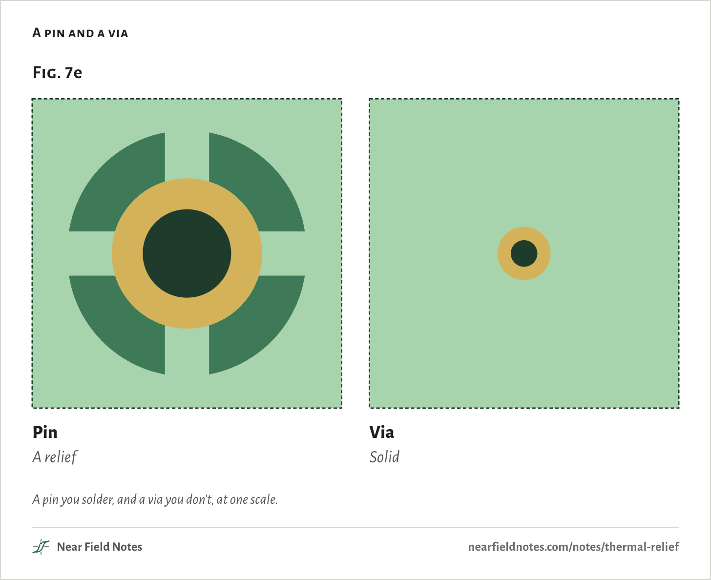
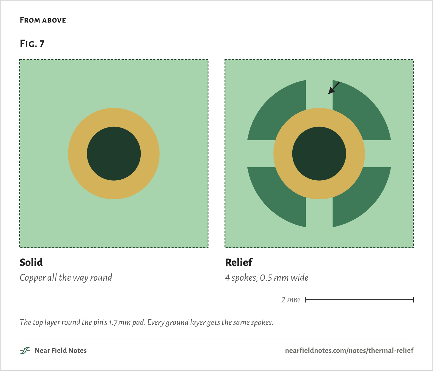
A through-hole ground pin’s pad sits in the ground copper on every layer it passes through. Tied in solid, that copper pulls the iron’s heat out sideways before the far side gets hot enough to melt the solder. A thermal relief cuts a gap round the pad and bridges it with a few thin spokes. KiCad’s default is four spokes 0.5 mm wide across a 0.5 mm gap.

From above
Fig. 7SolidCopper all the way roundRelief4 spokes, 0.5 mm wide2 mmFig. 7SolidCopper all the way roundRelief4 spokes, 0.5 mm wide2 mmFig. 7SolidCopper all the way roundRelief4 spokes, 0.5 mm wide2 mm

The top layer round the pin’s 1.7 mm pad. Every ground layer gets the same spokes.

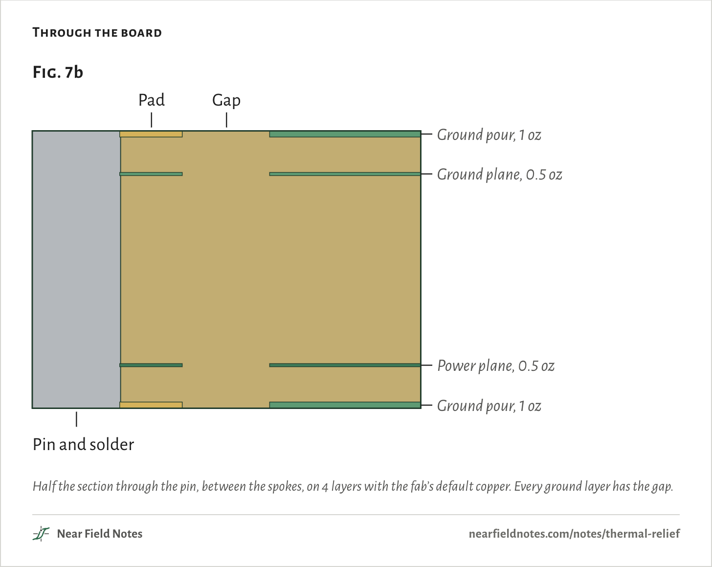
Through the board
Fig. 7bGround, 1 ozGround, 0.5 ozPower, 0.5 ozGround, 1 ozPadGapPin and solderFig. 7bGround pour, 1 ozGround plane, 0.5 ozPower plane, 0.5 ozGround pour, 1 ozPadGapPin and solderFig. 7bGround pour, 1 ozGround plane, 0.5 ozPower plane, 0.5 ozGround pour, 1 ozPadGapPin and solder

Half the section through the pin, between the spokes, on 4 layers with the fab’s default copper. Every ground layer has the gap.

How hot the iron has to be
  • Relief
  • Solid
Fig. 7cIron to melt the far side in 3 s, °C300350400450500550600650FX-888D’s top2 layers4753704 layers, fab default5364024 layers, 1 oz inside596434Fig. 7cIron to melt the far side in 3 s, °C300350400450500550600650FX-888D’s top2 layers4753704 layers, fab default5364024 layers, 1 oz inside596434Fig. 7cIron to melt the far side in 3 s, °C300350400450500550600650FX-888D’s top2 layers4753704 layers, fab default5364024 layers, 1 oz inside596434

The iron behind 7 K/W, taken for a 1.6 mm chisel tip with a solder bridge.

168

Set the iron yourself

3 boards, 300 to 500 °C
Board
400 °C
Thermal relief

4 layers, fab default, iron at 400 °C

  • Relief
  • Solid
  • Solder melts, 217 °C
Far side, °C05010015020025030035003691215Seconds with the iron onFar side, °C05010015020025030035003691215Seconds with the iron onFar side, °C05010015020025030035003691215Seconds with the iron on
Relief melts in
3.3 s
Solid melts in
Over 15 s

The far side of the same header pin, with the iron behind 7 K/W. The 4-layer board has the fab’s default copper.

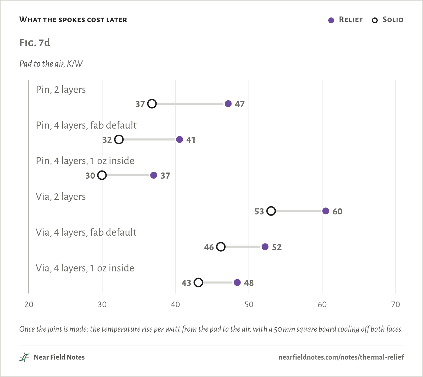
What the spokes cost later
  • Relief
  • Solid
Fig. 7dPad to the air, K/W203040506070Pin, 2 layers3747Pin, 4 layers, fab default3241Pin, 4 layers, 1 oz inside3037Via, 2 layers5360Via, 4 layers, fab default4652Via, 4 layers, 1 oz inside4348Fig. 7dPad to the air, K/W203040506070Pin, 2 layers3747Pin, 4 layers, fab default3241Pin, 4 layers, 1 oz inside3037Via, 2 layers5360Via, 4 layers, fab default4652Via, 4 layers, 1 oz inside4348Fig. 7dPad to the air, K/W203040506070Pin, 2 layers3747Pin, 4 layers, fab default3241Pin, 4 layers, 1 oz inside3037Via, 2 layers5360Via, 4 layers, fab default4652Via, 4 layers, 1 oz inside4348

Once the joint is made: the temperature rise per watt from the pad to the air, with a 50 mm square board cooling off both faces.

170

Where each belongs

Pins and vias
A pin and a via
Fig. 7ePinA reliefViaSolidFig. 7ePinA reliefViaSolidFig. 7ePinA reliefViaSolid

A pin you solder, and a via you don’t, at one scale.

172

Key to ground connections

Should this pad get a thermal relief?

  1. 1aNobody solders itSolid, like a via, 7e
  2. 1bIt gets solderedGo to 2
  3. 2aIt has to shed heatSolid, and a bigger iron
  4. 2bIt only needs a ground connectionA relief, 7e

KiCad puts reliefs on pads in a zone by default and ties vias in solid unless the zone is hatched.

173

Conditions

Board
50 by 50 mm, JLCPCB’s 1.6 mm stackups. On 4 layers, 0.2 mm of 7628 prepreg under each outer layer and a 1.065 mm core.
Copper
Ground poured on the outer layers, a ground plane on layer 2 and a power plane on layer 3. 1 oz outside, 0.5 oz inside as the fab’s default or 1 oz.
Pin
KiCad’s 2.54 mm header pad, 1.7 mm on a 1.0 mm hole, with a 0.64 mm brass pin and the rest of the hole full of SAC305. 20 µm of plating.
Via
0.6 mm on 0.3 mm, KiCad’s default, empty
Relief
KiCad’s zone default on every ground layer: 4 spokes 0.5 mm wide across a 0.5 mm gap
Iron
A fixed tip temperature behind 7 K/W, on the pad and the pin. 4 and 12 K/W move every number but never the order. A big chisel tip is about 4 K/W and a fine cone about 12.
Far side
The average over the bottom pad. Melted is 217 °C, where SAC305 starts to melt.
Solver
A 3D finite-volume heat model over a quarter of the board, 0.05 mm cells near the hole, stepped in time
Check
Halving the cells near the hole moves the steady K/W by 0.2%

Simulated only. Nothing on this page has been measured on a board yet.

Limits

  • Material properties don’t change with temperature, and the solder’s latent heat isn’t modeled. That keeps the model linear, so other iron settings are scaled from 350 °C runs.
  • The iron holds its tip temperature. A real tip cools as it pours heat in.
  • The pad is round and the spokes run along x and y.

Files

  • tsim/model.pyThe heat model
  • tsim/run.pyThe soldering runs, K/W and µΩ
  • tsim/iron.pyHow hot the iron has to be

Sources

Like this note?

Rev 1 ·
  1. Rev 1First published

Each fix gets a line here, with the reader's name if they want credit.

Did it answer your question?

Want more on this?

Report a problem

What should the next note be? Ask for one