Near Field Notes

Note 14Signal integrityRev 1Watch the video · 1:58

PHY and link layer

What does the PHY do, and what does the link layer do?

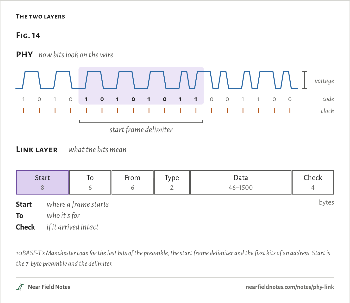
The PHY decides how bits look on the wire. It sets the voltages, the line code and where the clock comes from. The link layer decides what the bits mean. It marks where a frame starts, who it’s for and whether it arrived intact. Either one can change while the other stays.

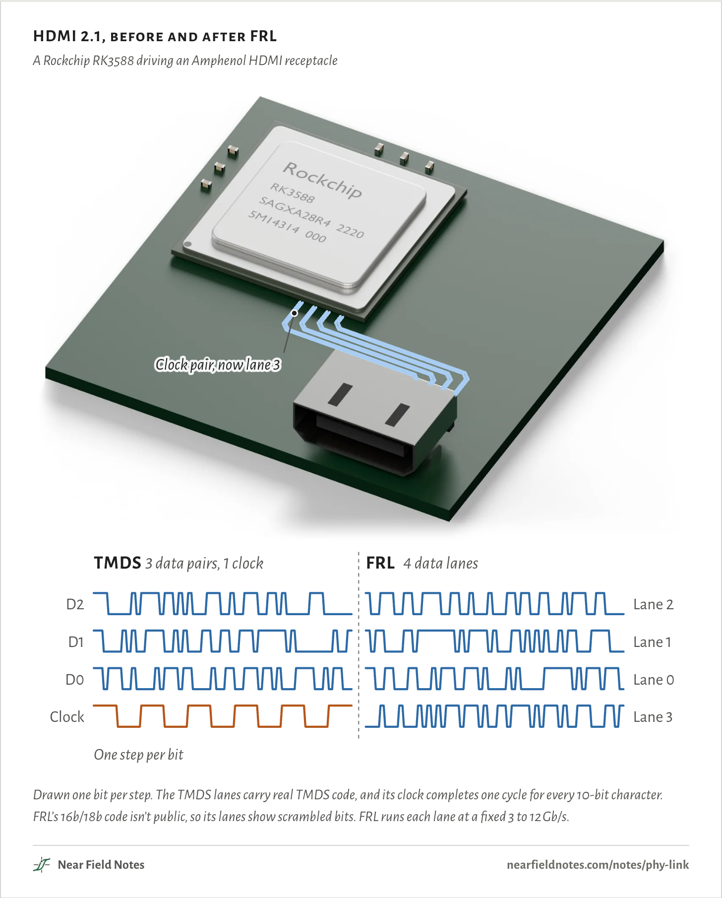
HDMI 2.1 shows the split. In its FRL mode, the old clock pair becomes a fourth data lane, and the clock rides inside the data, much as DisplayPort has done since its 2006 spec.

The figure sweeps the four pairs on a Rockchip RK3588 board through the old TMDS mode, then FRL.

HDMI 2.1, before and after FRL

A Rockchip RK3588 driving an Amphenol HDMI receptacle

Clock pair, now lane 3TMDSFRLD2Lane 2D1Lane 1D0Lane 0ClockLane 3One step per bitClock pair, now lane 3TMDSFRL3 data pairs, 1 clock4 data lanesD2Lane 2D1Lane 1D0Lane 0ClockLane 3One step per bitClock pair, now lane 3TMDSFRL3 data pairs, 1 clock4 data lanesD2Lane 2D1Lane 1D0Lane 0ClockLane 3One step per bit

Drawn one bit per step. The TMDS lanes carry real TMDS code, and its clock completes one cycle for every 10-bit character. FRL’s 16b/18b code isn’t public, so its lanes show scrambled bits. FRL runs each lane at a fixed 3 to 12 Gb/s.

Two layers

Layer 1 and layer 2

Every wired link splits its job in two. The physical layer, or PHY, moves raw bits. It sets the voltages, the line code that turns bits into levels, and how the far end finds the clock. The data link layer above it gathers the bits into frames, addresses them and checks them for errors.

The start of an Ethernet frame shows both. On 10BASE-T, every bit is an edge in the middle of its slot, rising for a 1 and falling for a 0, so the edges carry the clock as well. The link layer then reads 10101011 as the start of a frame.

The two layers
Fig. 14PHYhow bits look on the wirevoltage101010101011001100codeclockstart frame delimiterLink layerwhat the bits meanStart8To6From6Type2Data46–1500Check4bytesStartwhere a frame startsTowho it’s forCheckif it arrived intactFig. 14PHYhow bits look on the wirevoltage101010101011001100codeclockstart frame delimiterLink layerwhat the bits meanStart8To6From6Type2Data46–1500Check4bytesStartwhere a frame startsTowho it’s forCheckif it arrived intactFig. 14PHYhow bits look on the wirevoltage101010101011001100codeclockstart frame delimiterLink layerwhat the bits meanStart8To6From6Type2Data46–1500Check4bytesStartwhere a frame startsTowho it’s forCheckif it arrived intact

10BASE-T’s Manchester code for the last bits of the preamble, the start frame delimiter and the first bits of an address. Start is the 7-byte preamble and the delimiter.

Ethernet, in two chips

MAC, then PHY

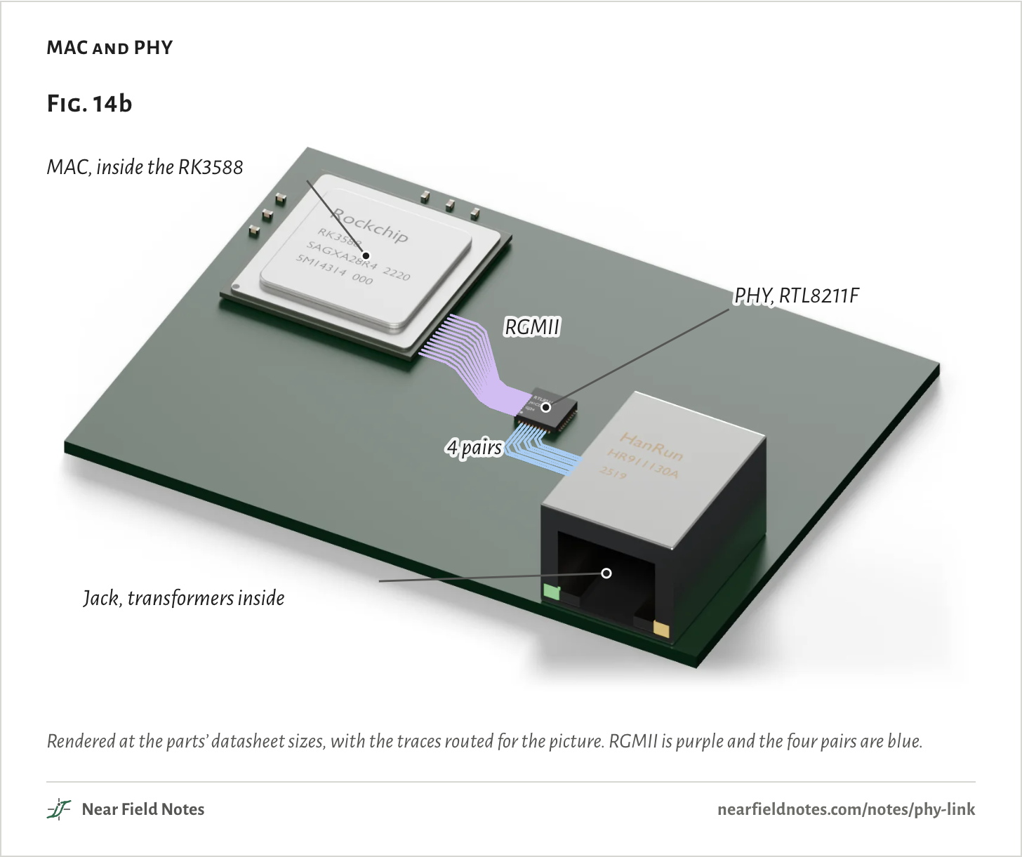
Ethernet often gives each layer a chip of its own. The MAC, the link layer, sits inside the processor and builds each frame. It hands the frame over RGMII to a separate PHY chip, which drives four twisted pairs through the jack’s transformers.

RGMII comes with a classic bring-up bug. Its clock has to arrive 1.5 to 2 ns after its data, and someone has to add that delay. The PHY can add it, or the MAC, or a longer trace.

MAC and PHY
Fig. 14bMAC, inside the RK3588PHY, RTL8211FJack, transformers insideRGMII4 pairsFig. 14bMAC, inside the RK3588PHY, RTL8211FJack, transformers insideRGMII4 pairsFig. 14bMAC, inside the RK3588PHY, RTL8211FJack, transformers insideRGMII4 pairs

Rendered at the parts’ datasheet sizes, with the traces routed for the picture. RGMII is purple and the four pairs are blue.

One frame, four PHYs

1980 to now

The frame the MAC builds has kept its fields since September 1980. They are the destination, source, type, data and a 32-bit check. The IEEE project for 800 Gb/s Ethernet committed to keeping them.

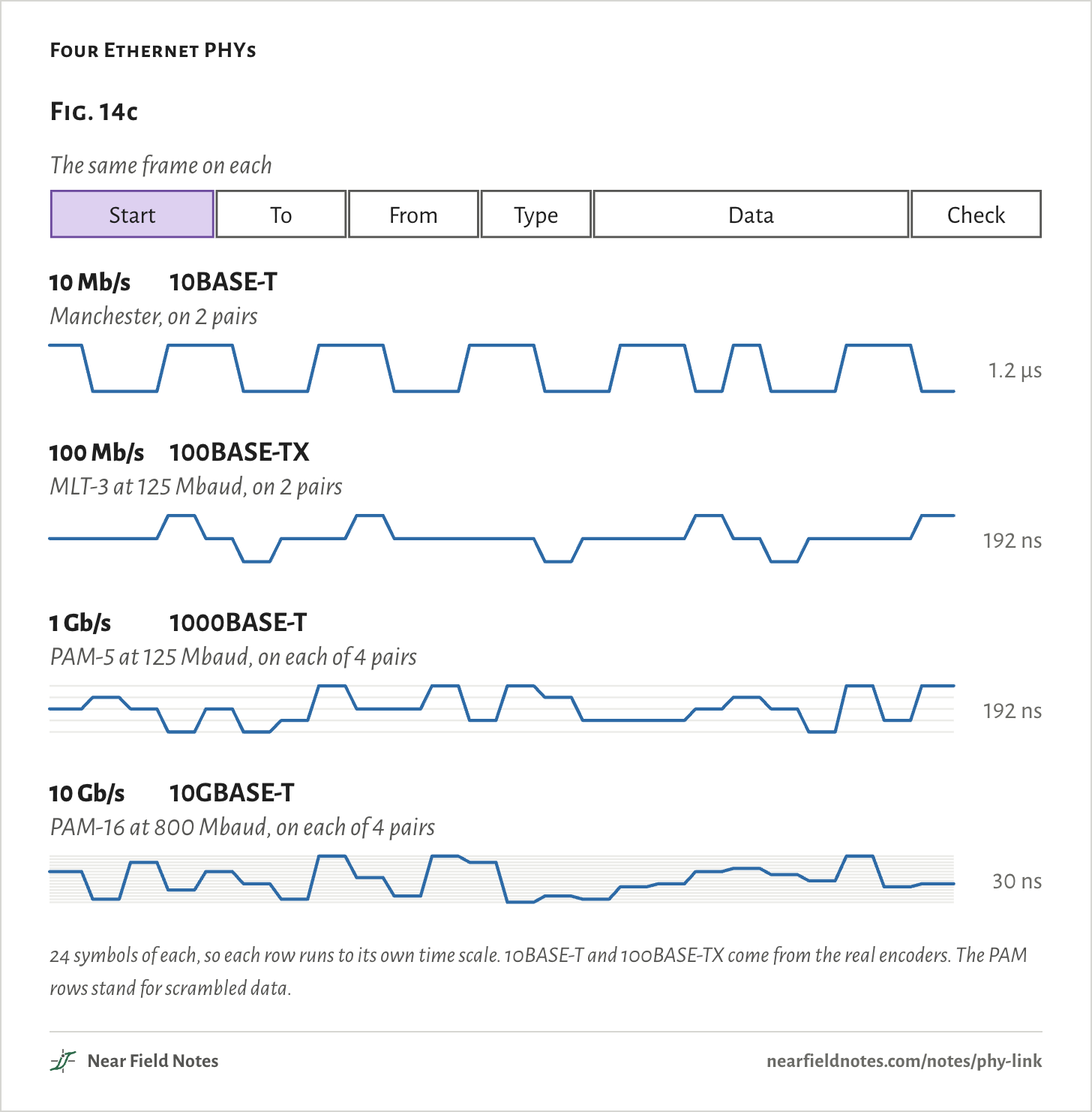
The PHY under it has been replaced again and again. 10BASE-T sends Manchester code. 100BASE-TX steps between three levels. Gigabit sends five levels on all four pairs, both ways at once, and 10GBASE-T sends sixteen at 800 Mbaud, with error correction on top.

Four Ethernet PHYs
Fig. 14cThe same frame on eachStartToFromTypeDataCheck10 Mb/s10BASE-TManchester, on 2 pairs1.2 µs100 Mb/s100BASE-TXMLT-3 at 125 Mbaud, on 2 pairs192 ns1 Gb/s1000BASE-TPAM-5 at 125 Mbaud, on each of 4 pairs192 ns10 Gb/s10GBASE-TPAM-16 at 800 Mbaud, on each of 4 pairs30 nsFig. 14cThe same frame on eachStartToFromTypeDataCheck10 Mb/s10BASE-TManchester, on 2 pairs1.2 µs100 Mb/s100BASE-TXMLT-3 at 125 Mbaud, on 2 pairs192 ns1 Gb/s1000BASE-TPAM-5 at 125 Mbaud, on each of 4 pairs192 ns10 Gb/s10GBASE-TPAM-16 at 800 Mbaud, on each of 4 pairs30 nsFig. 14cThe same frame on eachStartToFromTypeDataCheck10 Mb/s10BASE-TManchester, on 2 pairs1.2 µs100 Mb/s100BASE-TXMLT-3 at 125 Mbaud, on 2 pairs192 ns1 Gb/s1000BASE-TPAM-5 at 125 Mbaud, on each of 4 pairs192 ns10 Gb/s10GBASE-TPAM-16 at 800 Mbaud, on each of 4 pairs30 ns

24 symbols of each, so each row runs to its own time scale. 10BASE-T and 100BASE-TX come from the real encoders. The PAM rows stand for scrambled data.

Ethernet

IEEE 802.3

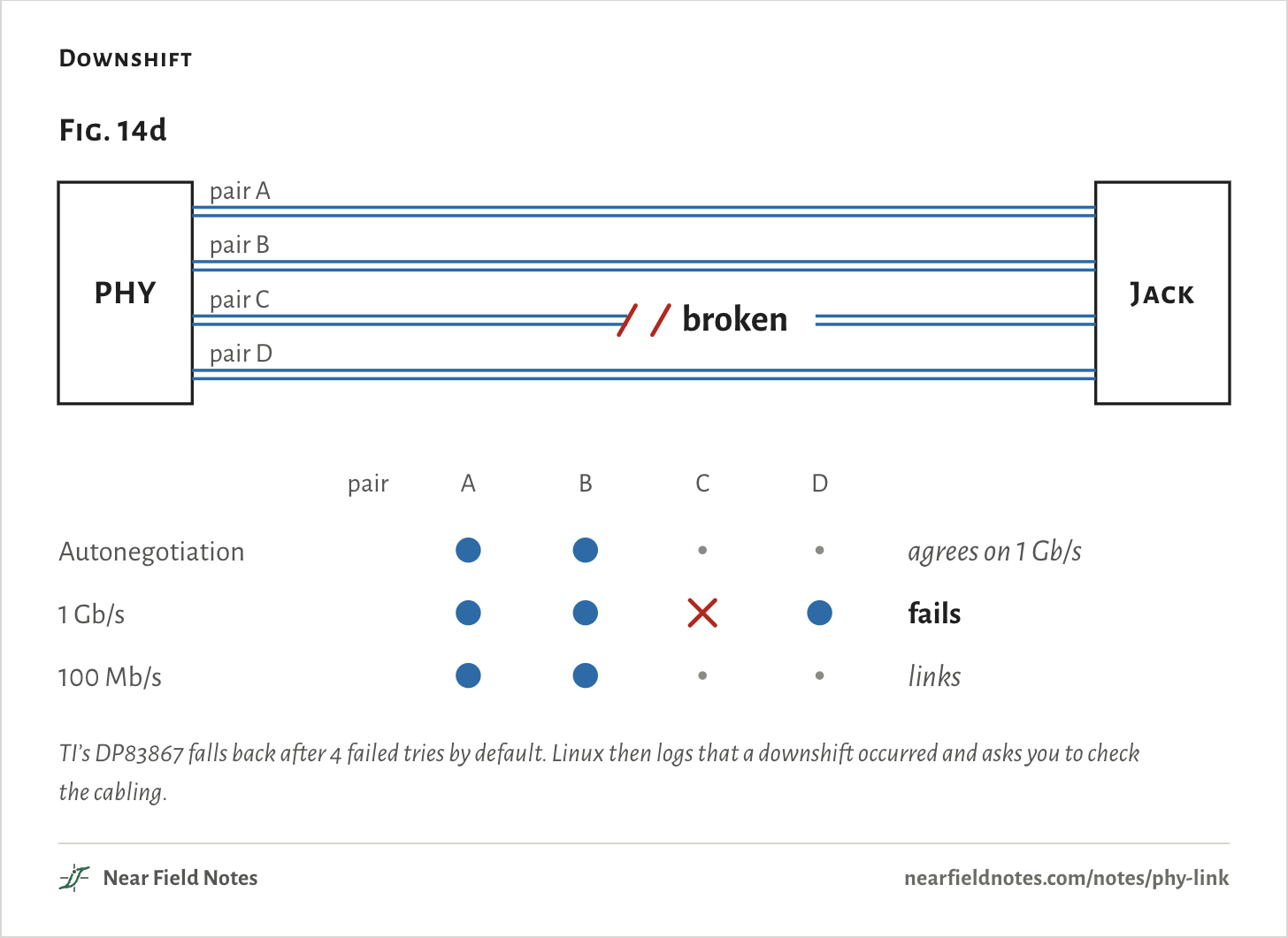
Gigabit needs all four pairs, A to D, but autonegotiation and 100 Mb/s use only A and B. So a cable with a break in pair C or D still agrees on 1 Gb/s, then fails to link.

Downshift
Fig. 14dPHYJackpair Apair Bbrokenpair Cpair DABCDpairAutonegotiationagrees on 1 Gb/s1 Gb/sfails100 Mb/slinksFig. 14dPHYJackpair Apair Bbrokenpair Cpair DABCDpairAutonegotiationagrees on 1 Gb/s1 Gb/sfails100 Mb/slinksFig. 14dPHYJackpair Apair Bbrokenpair Cpair DABCDpairAutonegotiationagrees on 1 Gb/s1 Gb/sfails100 Mb/slinks

TI’s DP83867 falls back after 4 failed tries by default. Linux then logs that a downshift occurred and asks you to check the cabling.

290

One PHY, a choice of link layers

Combo PHYs

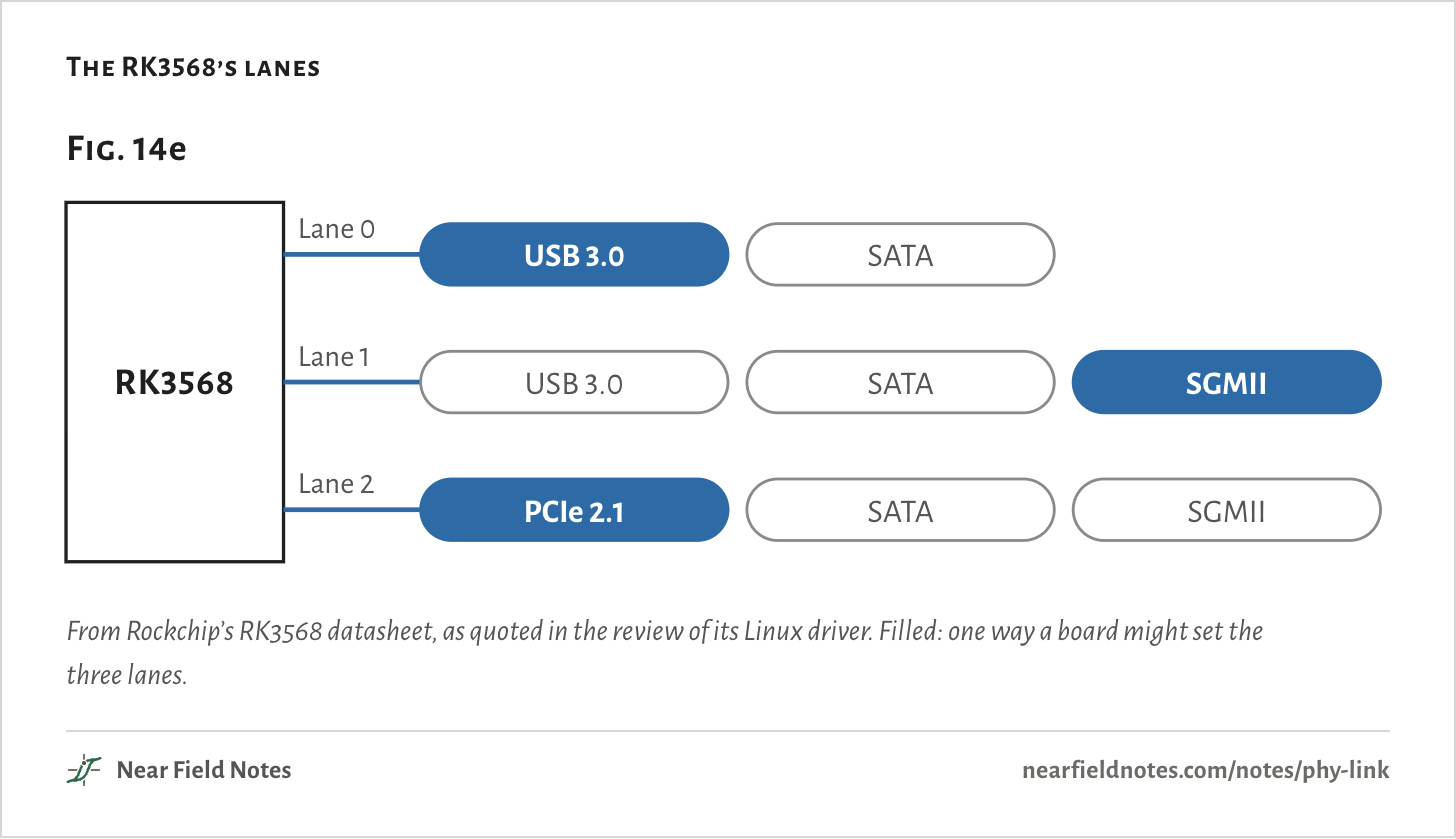
Some chips turn it around, with one PHY and a choice of link layers on top. Each of the Rockchip RK3568’s three SerDes lanes can be one of two or three interfaces, and the board picks which.

It’s one job per lane. A board that uses lane 2 for PCIe gives up SATA and SGMII on it.

The RK3568’s lanes
Fig. 14eRK3568Lane 0USB 3.0SATALane 1USB 3.0SATASGMIILane 2PCIe 2.1SATASGMIIFig. 14eRK3568Lane 0USB 3.0SATALane 1USB 3.0SATASGMIILane 2PCIe 2.1SATASGMIIFig. 14eRK3568Lane 0USB 3.0SATALane 1USB 3.0SATASGMIILane 2PCIe 2.1SATASGMII

From Rockchip’s RK3568 datasheet, as quoted in the review of its Linux driver. Filled: one way a board might set the three lanes.

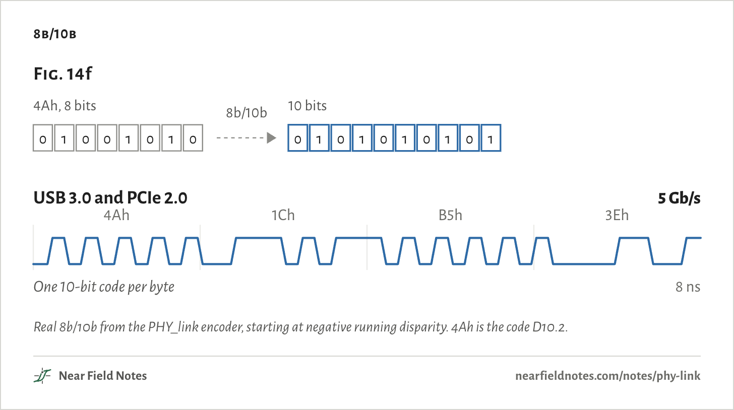
It works because those PHYs are close cousins. USB 3.0 shares PCIe 2.0’s signaling. Both run at 5 Gb/s, with the same 8b/10b code carrying the clock. Intel’s PIPE spec, begun for PCIe in 2002, now gives one PHY interface for PCIe, SATA, USB, DisplayPort and USB4.

8b/10b turns each byte into one of a set of 10-bit codes, chosen to keep the line balanced and full of edges for the clock. The byte 4Ah becomes 0101010101.

8b/10b
Fig. 14f4Ah, 8 bits010010108b/10b: 10 bits0101010101USB 3.0 and PCIe 2.05 Gb/s4Ah1ChB5h3Eh8 nsOne 10-bit code per byteFig. 14f4Ah, 8 bits010010108b/10b10 bits0101010101USB 3.0 and PCIe 2.05 Gb/s4Ah1ChB5h3Eh8 nsOne 10-bit code per byteFig. 14f4Ah, 8 bits010010108b/10b10 bits0101010101USB 3.0 and PCIe 2.05 Gb/s4Ah1ChB5h3Eh8 nsOne 10-bit code per byte

Real 8b/10b from the PHY_link encoder, starting at negative running disparity. 4Ah is the code D10.2.

MIPI CSI-2

One link layer, two PHYs

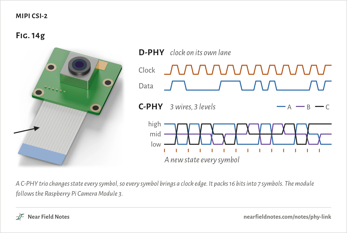
The reverse happens too, with one link layer on different PHYs. A phone camera’s CSI-2 link can run on a D-PHY, which sends its clock on a lane of its own, or on a C-PHY, which uses three wires per lane at three levels and builds the clock in.

MIPI CSI-2
Fig. 14gD-PHYclock on its own laneClockDataC-PHY3 wires, 3 levelsABChighmidlowA new state every symbolFig. 14gD-PHYclock on its own laneClockDataC-PHY3 wires, 3 levelsABChighmidlowA new state every symbolFig. 14gD-PHYclock on its own laneClockDataC-PHY3 wires, 3 levelsABChighmidlowA new state every symbol

A C-PHY trio changes state every symbol, so every symbol brings a clock edge. It packs 16 bits into 7 symbols. The module follows the Raspberry Pi Camera Module 3.

292

Bluetooth LE

Three PHYs, one link

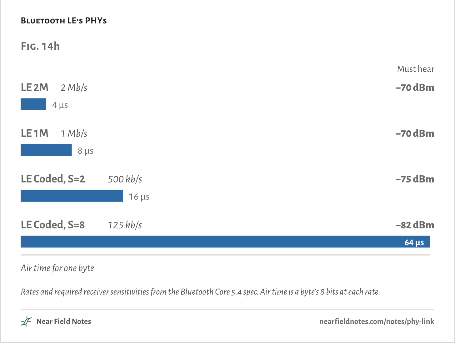
A radio link can even change PHY while it runs. Bluetooth LE has three. LE 1M is the original. LE 2M is twice as fast, and LE Coded spends 2 or 8 symbols on every bit to reach farther.

Bluetooth LE’s PHYs
Fig. 14hMust hearLE 2M2 Mb/s−70 dBm4 µsLE 1M1 Mb/s−70 dBm8 µsLE Coded, S=2500 kb/s−75 dBm16 µsLE Coded, S=8125 kb/s−82 dBm64 µsAir time for one byteFig. 14hMust hearLE 2M2 Mb/s−70 dBm4 µsLE 1M1 Mb/s−70 dBm8 µsLE Coded, S=2500 kb/s−75 dBm16 µsLE Coded, S=8125 kb/s−82 dBm64 µsAir time for one byteFig. 14hMust hearLE 2M2 Mb/s−70 dBm4 µsLE 1M1 Mb/s−70 dBm8 µsLE Coded, S=2500 kb/s−75 dBm16 µsLE Coded, S=8125 kb/s−82 dBm64 µsAir time for one byte

Rates and required receiver sensitivities from the Bluetooth Core 5.4 spec. Air time is a byte’s 8 bits at each rate.

294

CAN

The wire picks who talks

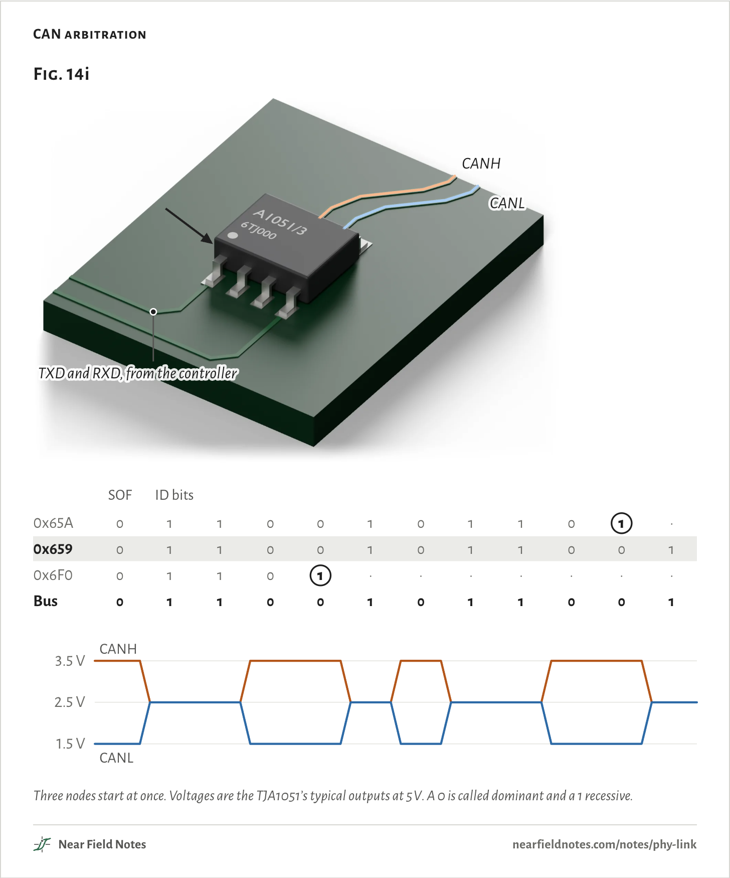
On CAN, the PHY even settles who may talk. A transceiver drives the bus for a 0 and lets it rest for a 1, so when two nodes send at once, the bus shows the 0.

Each node reads the bus back as it sends its ID. One that sends a 1 and reads a 0 has lost, and goes quiet. The lowest ID wins, and its frame carries on untouched.

CAN arbitration
Fig. 14iCANHCANLTXD and RXD, from the controllerSOFID bits0x65A01100101101·0x6590110010110010x6F001101·······Bus0110010110011.5 V2.5 V3.5 VCANHCANLFig. 14iCANHCANLTXD and RXD, from the controllerSOFID bits0x65A01100101101·0x6590110010110010x6F001101·······Bus0110010110011.5 V2.5 V3.5 VCANHCANLFig. 14iCANHCANLTXD and RXD, from the controllerSOFID bits0x65A01100101101·0x6590110010110010x6F001101·······Bus0110010110011.5 V2.5 V3.5 VCANHCANL

Three nodes start at once. Voltages are the TJA1051’s typical outputs at 5 V. A 0 is called dominant and a 1 recessive.

296

HDMI

DVI with sound

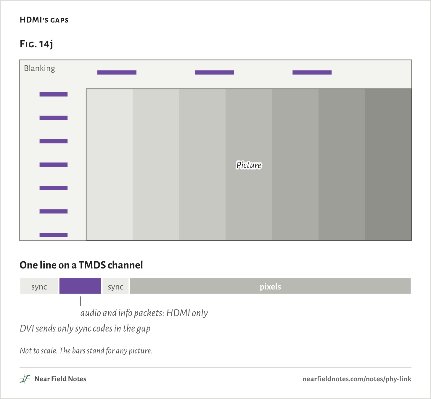
HDMI began as DVI. HDMI 1.0, final in December 2002, kept DVI’s TMDS PHY. That’s three data pairs and a clock pair, each line pulled up to 3.3 V through 50 Ω at the screen. Its link layer added sound, in packets fitted into the gaps between lines and frames.

HDMI’s gaps
Fig. 14jPictureBlankingOne line on a TMDS channelpixelsaudio and info packets: HDMI onlyDVI sends only sync codes in the gapFig. 14jPictureBlankingOne line on a TMDS channelsyncpixelsaudio and info packets: HDMI onlyDVI sends only sync codes in the gapFig. 14jPictureBlankingOne line on a TMDS channelsyncsyncpixelsaudio and info packets: HDMI onlyDVI sends only sync codes in the gap

Not to scale. The bars stand for any picture.

298

DisplayPort

On four kinds of wire

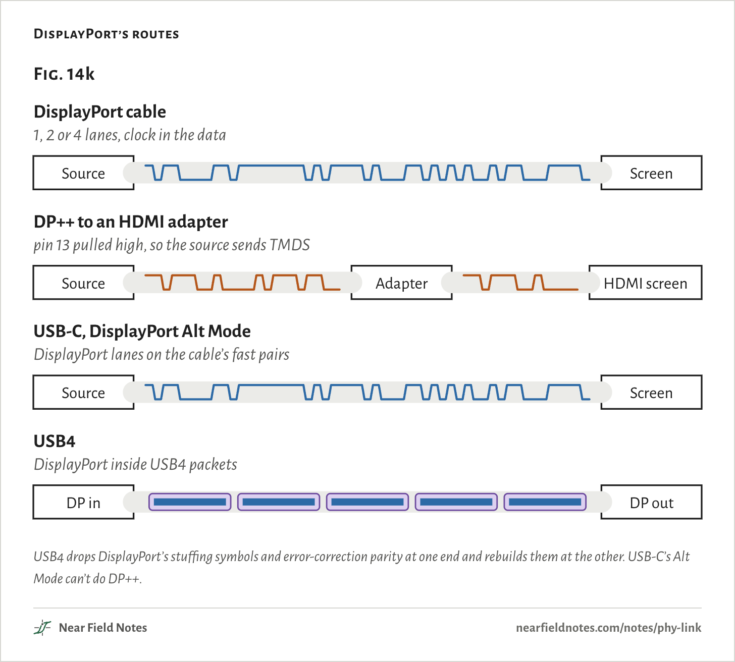
DisplayPort started from a link with no clock wire. It has 1, 2 or 4 lanes that carry the clock in the data, AC-coupled at 400 mV by default, and a slow side channel, AUX, for setup. It has since run on PHYs that aren’t its own.

DisplayPort’s routes
Fig. 14kDisplayPort cable1, 2 or 4 lanes, clock in the dataSourceScreenDP++ to an HDMI adapterpin 13 pulled high, so the source sends TMDSSourceAdapterScreenUSB-C, DisplayPort Alt ModeDisplayPort lanes on the cable’s fast pairsSourceScreenUSB4DisplayPort inside USB4 packetsDP inDP outFig. 14kDisplayPort cable1, 2 or 4 lanes, clock in the dataSourceScreenDP++ to an HDMI adapterpin 13 pulled high, so the source sends TMDSSourceAdapterHDMI screenUSB-C, DisplayPort Alt ModeDisplayPort lanes on the cable’s fast pairsSourceScreenUSB4DisplayPort inside USB4 packetsDP inDP outFig. 14kDisplayPort cable1, 2 or 4 lanes, clock in the dataSourceScreenDP++ to an HDMI adapterpin 13 pulled high, so the source sends TMDSSourceAdapterHDMI screenUSB-C, DisplayPort Alt ModeDisplayPort lanes on the cable’s fast pairsSourceScreenUSB4DisplayPort inside USB4 packetsDP inDP out

USB4 drops DisplayPort’s stuffing symbols and error-correction parity at one end and rebuilds them at the other. USB-C’s Alt Mode can’t do DP++.

300

Back to HDMI 2.1

Lanes alike, wires apart

FRL brought HDMI close to DisplayPort in structure. It has up to four lanes with the clock in the data, a few fixed rates, link training and Reed-Solomon error correction.

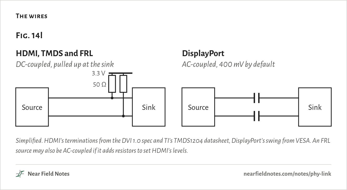
Its wires stayed HDMI’s. The sink still pulls each line up to 3.3 V, where DisplayPort couples through capacitors. They are close enough for one PHY to do both. The RK3588’s Samsung-designed PHY drives either HDMI 2.1 at up to 12 Gb/s a lane or a laptop panel’s eDP, picked by its driver each time it powers on.

The wires
Fig. 14lHDMI, TMDS and FRLDC-coupled, pulled up at the sinkSourceSink3.3 V50 ΩDisplayPortAC-coupled, 400 mV by defaultSourceSinkFig. 14lHDMI, TMDS and FRLDC-coupled, pulled up at the sinkSourceSink3.3 V50 ΩDisplayPortAC-coupled, 400 mV by defaultSourceSinkFig. 14lHDMI, TMDS and FRLDC-coupled, pulled up at the sinkDisplayPortAC-coupled, 400 mV by defaultSourceSink3.3 V50 ΩSourceSink

Simplified. HDMI’s terminations from the DVI 1.0 spec and TI’s TMDS1204 datasheet, DisplayPort’s swing from VESA. An FRL source may also be AC-coupled if it adds resistors to set HDMI’s levels.

Side by side

Every link on this page
PHYs and link layers
LinkPHYCodeRateClock
Ethernet10BASE-TManchester10 Mb/s on 2 pairsIn the data
Ethernet100BASE-TX4B5B, then MLT-3125 Mbaud on 2 pairsIn the data
Ethernet1000BASE-TPAM-5250 Mb/s on each of 4 pairsIn the data
Ethernet10GBASE-TPAM-16 with LDPC800 Mbaud on each of 4 pairsIn the data
USB 3.0SuperSpeed8b/10b5 Gb/sIn the data
PCIe 2.0Gen 28b/10b5 Gb/sIn the data
MIPI CSI-2D-PHYBits on each laneUp to 3.2 Gb/s a lane in one coreIts own lane
MIPI CSI-2C-PHY16 bits in 7 symbolsAbout 2.28 bits a symbolIn the data
Bluetooth LELE 1M, LE 2M, LE CodedNone, or 2 or 8 symbols a bit125 kb/s to 2 Mb/sIn the data
CANISO 11898-2A stuff bit after 5 equal bits1 Mb/s, CAN FD data to 5 Mb/sOn the edges
HDMI, DVITMDS8 bits to 10Up to 1.65 Gb/s a pair on one DVI linkIts own pair
HDMI 2.1FRL16b/18b3 to 12 Gb/s on 3 or 4 lanesIn the data
DisplayPortMain link8b/10b1.62, 2.7, 5.4 or 8.1 Gb/s a laneIn the data
DisplayPort 2.xUHBR128b/132b10, 13.5 or 20 Gb/s a laneIn the data
DisplayPortUSB4’s, tunneledUSB4 packetsShares the USB4 linkUSB4’s

Rates are per lane or pair where a link has several. Every entry is sourced below.

Read the two layers apart and the odd cases add up. Ethernet keeps one frame on ever faster PHYs. One PHY serves several link layers. DisplayPort’s link layer rides whichever PHY reaches the screen.

Conditions

Method
No simulation. Each waveform is the bits or symbols that PHY sends, from the PHY_link project’s encoders.
Exact codes
10BASE-T’s Manchester, 100BASE-TX’s 4B5B, scrambler and MLT-3, DVI’s TMDS, 8b/10b, CAN arbitration and C-PHY’s wire states
Levels only
1000BASE-T’s PAM-5, 10GBASE-T’s PAM-16 and HDMI’s FRL, as scrambled data
Renders
Blender, with parts at their datasheet sizes: Rockchip RK3588, Amphenol 10029449-111RLF, Realtek RTL8211F, HanRun HR911130A, NXP TJA1051T/3 and a module after the Raspberry Pi Camera Module 3. Traces are routed for the picture.
Claims
Each one checked against its source in the project’s research notes, with datasheet values from NXP, Microchip and the DVI 1.0 spec

Drawn from specs and datasheets. Nothing on this page was measured.

Limits

  • The waveforms are ideal symbols with smooth edges, not what arrives after a cable.
  • HDMI’s spec isn’t public. Its packets in the gaps are described from a Sony patent, and FRL from test-equipment and IP vendors.
  • Downshift is a vendor feature. Realtek’s datasheet doesn’t mention it, though Linux supports it on the RTL8211F.
  • The RK3588’s combo PHY drives HDMI or eDP. Its external DisplayPort comes from a different PHY.
  • The D-PHY rates are one vendor’s core, not the spec’s limits.

Files

  • sim/linecodes.pyThe encoders behind every waveform
  • render/scene.pyThe renders
  • refs/research.md57 checked claims and their sources
  • anim/hook.pyThe video these figures come from

Sources

Like this note?

Rev 1 ·
  1. Rev 1First published

Each fix gets a line here, with the reader's name if they want credit.

Did it answer your question?

Want more on this?

Report a problem

What should the next note be? Ask for one